
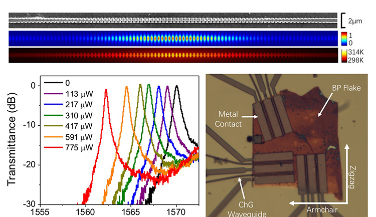
 Top: Top-view SEM micrograph, electromagnetic field and thermal profile of graphene-sandwiched photonic crystal thermo-optic switch. Bottom left: Resonance shifts of the switch under different input power. Bottom right: Mid-IR, waveguide-integrated black-phosphorus photodetectors. [Enlarge figure]
Since graphene’s discovery in 2004, hundreds of 2-D materials have been synthesized. These materials exhibit a wide range of properties spanning the entire optical spectrum, which makes them tantalizing choices for enabling novel photonic functions. In the past year, we have demonstrated a material integration scheme that could make the unique properties of 2-D materials more accessible for photonic applications.
Currently, most photonic devices using 2-D materials are fabricated by a hybrid transfer process, which relies on delamination and attachment of these atomically thin crystals onto prefabricated photonic devices. Despite its widespread adoption, this approach offers limited yield, and light can interact with the 2-D materials only through the relatively weak evanescent wave. A monolithic integration approach, defining photonic circuits directly on top of the 2-D materials, could overcome these disadvantages. But direct deposition of optically thick dielectric materials onto 2-D crystals has been challenging, owing to poor adhesion with their hydrophobic surfaces and to lattice defects often introduced into the process.
We have recently pioneered a monolithic 2-D material integration scheme capitalizing on chalcogenide glasses (ChGs)—amorphous compounds of sulfur, selenium or tellurium.1 Unlike many other dielectrics, which require high temperature or a plasma state during deposition, ChG films can be formed at room temperature, allowing preservation of the 2-D materials’ structural integrity and optoelectronic properties.
The new integration scheme has enabled unconventional multilayer structures to optimize light-matter interactions in 2-D layers. Further, we have shown that the multifunctional ChG material can simultaneously act as a low-loss light-guiding medium (with broadband transparency from the visible to the mid-infrared), a gate dielectric to modulate Fermi levels in 2-D materials, and a passivation layer to effectively inhibit degradation of less stable 2-D materials such as black phosphorus.
Leveraging this new integration strategy, we realized a series of photonic devices,1 including a waveguide polarizer with an octave-spanning bandwidth using a novel graphene-sandwiched structure, an on-chip thermo-optic switch with record energy efficiency, and a mid-IR graphene modulator using infrared-transparent ChG as the gate material. We also demonstrated the first mid-IR waveguide-integrated photodetector based on black phosphorus.2 In this last example, we further leveraged our integration approach to precisely align photonic devices and 2-D crystals with lithographic accuracy, and quantified the orientation-dependent in-plane photodetection response of black phosphorus.
Our team and collaborators are now working on expanding the technology to facilitate the integration of many more classes of 2-D materials. With the significantly simplified fabrication process and unconventional device geometries previously inaccessible using classical hybrid bonding, the ChG-on-2-D-material platform is, we believe, poised to significantly expedite and expand integration of 2-D materials to enable new photonic functionalities.
Researchers
Hongtao Lin, Zhejiang University, Hangzhou, China
Skylar Deckoff-Jones and Juejun Hu, Massachusetts Institute of Technology, Cambridge, Mass., USA
References
1. H. Lin et al. Nat. Photon. 11, 798-805 (2017).
2. S. Deckoff-Jones et al. J. Opt. 20, 044004 (2018).