
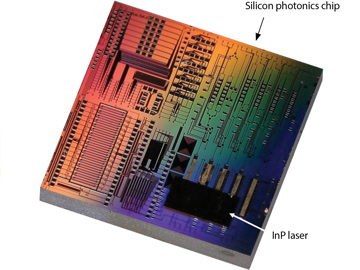
 Silicon photonics chip with 3-D hybrid integrated InP laser array.
More than US$1 billion and years of research and development have been invested in “photonizing” silicon—adding photonics to silicon CMOS processes, to leverage the tools available in the microelectronics industry for high yield and low cost. The photonics industry’s mindset has been traditionally vertical; companies carry out most design, fabrication, back-end processing and packaging in-house, to protect intellectual property. Previous attempts to standardize and share processes have failed, but the landscape is changing, with the emergence of foundries offering silicon photonics processes and “fabless” photonics companies utilizing those foundry processes.
Whatever ultimately drives fabrication technology, little doubt exists that silicon photonics is poised to revolutionize information transfer and will profoundly impact a range of industries. Yet integrated laser sources remain a bottleneck for silicon photonics. This year, we demonstrated a 3-D hybrid laser integration approach that is scalable, low cost and reliable, with superior thermal performance.1-4
Laser integration approaches for silicon photonics can be categorized as monolithic, heterogenous or hybrid. Monolithic approaches involve the direct hetero-epitaxy of laser materials, such as compound semiconductors, on silicon. This approach is the least mature. Heterogeneous approaches involve the intimate merging of traditionally incompatible materials and their subsequent co-fabrication to form devices. This allows for best-in-class materials selection—but also requires complex fabrication processes.
Hybrid integration, the third approach, is the most mature. One example, co-packaging, uses micro-optics to couple laser light to silicon waveguides. Another, more scalable hybrid approach involves butt-coupling of lasers and silicon waveguides without the use of micro-optics—accomplished by mounting two chips side by side on a common carrier, or by flip-chip bonding of laser chips into recesses adjacent to silicon waveguides.
We believe the most promising approaches for realizing lasers on silicon are hybrid approaches that add the laser in a back-end step, thereby avoiding the requirement to co-fabricate incompatible materials and allowing separate, optimized fabrication of the silicon photonic integrated circuit and laser sources. The 3-D integration that we demonstrated this year takes such a hybrid approach, based on flip-chip bonding and vertical coupling between indium phosphide (InP) and silicon waveguides. For the InP waveguide, vertical emission is achieved with a total-internal-reflection turning mirror. For the silicon waveguide, a grating coupler achieves vertical coupling. The InP chip is flip-chip bonded directly to the silicon substrate, providing an effective heat sink. With high coupling efficiency, low cost and superior thermal performance, these 3-D hybrid lasers show promise for future large-scale integrated silicon photonics.
Researchers
Jonathan Klamkin and Bowen Song, University of California, Santa Barbara, Calif., USA
References
1. B. Song et al. Opt. Express 24, 10435 (2016).
2. B. Song et al. Conference on Lasers and Electro-Optics paper SM4G.5 (2016).
3. B. Song et al. European Conference on Optical Communication paper We2.5.5 (2015).
4. P. Contu et al. IEEE Photonics Conference paper Tue3.2 (2014).