
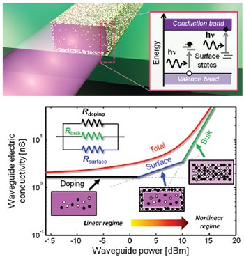
 (Top) Massive, light-induced free-carrier generation on the surface of Si photonic waveguides. (Bottom) Light-dependent electric conductivity of a 1-mm-long Si waveguide. At moderate light intensity (0–10 dBm), the surface contribution is dominant.
Recently, great efforts have been devoted to shrinking the size of optoelectronic devices down to the nanoscale. However, the optical and electrical properties of nanoscale devices are strongly affected by the nature of their surfaces, where physical phenomena not occurring in the bulk material may appear. The electrical conductivity in semiconductor nanomembranes and nanowires, for example, is dominated by surface contributions.1
In our research, we found a similar behavior for silicon (Si) photonic nanowaveguides in the presence of light.2 When near-infrared light (for example, around 1,550 nm wavelength) propagates in Si waveguides, many electrical free carriers are generated at the core–cladding interface. This effect, a by-product of natural surface states, results from absorption of photons with energy lower than the 1.12-eV band gap of bulk Si. This photogeneration phenomenon is unexpectedly massive; in fact, only 1 mW of optical power is enough to generate 100 times more surface free carriers than the carrier density thermally available in the bulk of the waveguide for the conventional doping level (1015 cm–3), and 10,000 times more than the number generated by conventional two-photon absorption.
This effect implies that, at light intensity typical of linear applications, the surface of Si nanowaveguides becomes highly conductive, exhibiting a metal-like behavior. That pattern has a twofold impact: the electric conductivity of the surface overwhelms that of the bulk Si; and an additional absorption mechanism arises, which we have named surface free-carrier absorption (SCA).
A more realistic picture of Si nanowaveguides thus emerges, with information on how to inhibit or enhance waveguide surface effects. These should be more significant as the waveguide size is reduced, with a maximum impact on subwavelength structures, such as nanoplasmonic devices, where the waveguide size approaches that of its own surface. Also, surface effects will play a key role in ultracompact electrooptic devices such as high-speed modulators, where the real electric resistance of the Si waveguide needs to be considered.
We expect our results to apply also to other semiconductor photonic technologies, such as InP, Ge and GaAs and their compounds. The energy gap of the core material relative to the photon wavelength, the properties of the cladding material, and the quality of the core–cladding interface all help determine the impact of surface effects. Ultimately, the waveguide surface matters much more than one could suspect.
Researchers
Stefano Grillanda and Francesco Morichetti, Politecnico di Milano, Italy
References
1. P. Zhang et al. Nature 439, 703 (2006).
2. S. Grillanda and F. Morichetti. Nat. Commun. 6, 8182 (2015).