
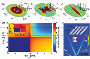
 (Top) Longitudinal electric field of SPPs propagating along (a) elliptic, (b) hyperbolic, and (c) σ-near-zero metasurfaces. Insets present corresponding isofrequency contours. (d) Calculated SER of a z-oriented dipole located above a metasurface, whose conductivity components are varied to explore all dispersion topologies, including elliptic (first and third quadrants) and hyperbolic (second and forth quadrants). Inset details topological transition offering maximum SER enhancement. (e) Implementation of hyperbolic metasurfaces using nanostructured graphene (top), with calculated SPP power flow. [Adapted from J.S. Gomez-Diaz et al., Phys. Rev. Lett. 114, 233901 (2015)]
Metamaterials offer unusual light–matter interactions that allow manipulation of wave propagation in unusual ways. Practical examples include permittivity-near-zero (ENZ) and hyperbolic metamaterials (HMTMs), which have enabled applications such as hyperlensing, negative refraction, and broadband, giant enhancement of the spontaneous emission rate (SER) of nearby emitters.1 Fabrication challenges and volumetric losses, however, have so far hindered the applicability of ENZ and HMTMs in optics. These challenges can be overcome by introducing ultrathin metasurfaces that provide superior electromagnetic performance over an ultrathin, planarized and easily accessible platform that is fully compatible with optoelectronic components and circuit integration.2
By merging the concepts of ENZ, HMTMs and 2-D materials, we recently proposed ultrathin uniaxial metasurfaces supporting hyperbolic plasmon propagation and extreme conductivity responses.3 An experimental realization at visible frequencies using single-crystal silver nanostructures has also been recently reported.4
Compared with surface plasmon polaritons (SPPs) propagating over conventional surfaces characterized by elliptic propagation properties, hyperbolic plasmons are guided toward specific directions in the plane (see figure). Ideally they are confined well below diffraction (with the confinement limited in practice only by losses and granularity) and support a strong enhancement of the local density of states. In addition, extremely anisotropic conductivity-near-zero metasurfaces support dispersion-free SPPs and the canalization regime typical of volumetric ENZ structures.5
In contrast to waves propagating in bulk media, plasmons possess evanescent fields in the direction perpendicular to the metasurface, offering more resilience to losses and a dramatic enhancement of light–matter interactions, reaching the maximum at the topological transition between closed elliptic and open hyperbolic regimes. We envision that nanostructured graphene, modeled by an effective conductivity tensor, can realize dynamic metasurfaces that are able to modify their dispersion topology by applying a gate bias, thus tuning topological transitions in real time.
These structures can pave the way toward ultrathin devices able to strongly interact with incoming light, allowing dynamic processing of extremely confined and easily accessible SPPs, and thereby enabling exciting applications in imaging, sensing, quantum optics and on-chip networks.
Researchers
J. Sebastian Gomez-Diaz, Mykhailo Tymchenko and Andrea Alù, University of Texas at Austin, Austin, Texas, USA
References
1. A. Poddubny et al. Nat. Photon. 7, 948 (2013).
2. N. Yu et al. Nat. Mater. 13, 139 (2014).
3. J.S. Gomez-Diaz et al. Phys. Rev. Lett. 114, 233901 (2015).
4. A.A. High et al. Nature 522, 192 (2015).
5. E. Forati et al. Phys. Rev. B 89, 081410 (2014).