
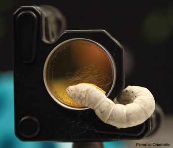
 Image of a Bombyx mori caterpillar spinning silk on the surface of a gold mirror. The “silkworms” spin nearly 1 km of silk in a “figure 8” pattern (visible on the surface of the mirror) to form their cocoons.
Silk fibers have woven their way through thousands of years of history, in the fabric of kings, the protective drapes of warriors, the clothing of fashion models. As a trade commodity, this material once defined the world economy along a “silk road” extending from ancient China through Samarkand (modern Uzbekistan) to the shores of Europe and beyond. Silk’s distinctive feel and shine, as well as its combination of unusual strength and toughness, have made it a coveted material across generations.
But silk is also finding new uses in some surprising places. Blessed with superb and versatile optical properties, physically robust and rooted in a natural biological system, this material can be fashioned into a range of micro- and nanoscale devices for drug delivery, disease diagnosis and biomedical sensing. As a result, the unlikely combination of silk, optics and biology is emerging as a new and potentially powerful tool in the drive toward personalized medicine.
Reverse-engineering a natural material
Although fit to clothe royalty, silk has the most humble beginnings imaginable. Inside the body of the silkworm caterpillar, Bombyx mori, digested mulberry leaves provide raw material for the synthesis of silk protein. The silk gland of the silkworm, which constitutes a large share of the insect’s volume, contains a mixture of silk fibroin protein, salts and water, which is extruded through a spinneret and drawn into a long, thin fiber as the caterpillar spins its cocoon and prepares to transform into a moth.
The fibers in the silk cocoon are very different from the liquid protein solution found within the silk gland. The fibers are long, thin, opaque, flexible and tough—ideal for a cocoon (or a silk scarf), but unworkable in optical devices. Using silk in optical devices requires reverse engineering of the natural fiber generation process, dissolving the native silk fibers to obtain a purified silk solution (water and fibroin) that closely resembles the material in the caterpillar’s silk gland. This versatile solution forms the starting material for silk films, gels, sponges, blocks and other materials.
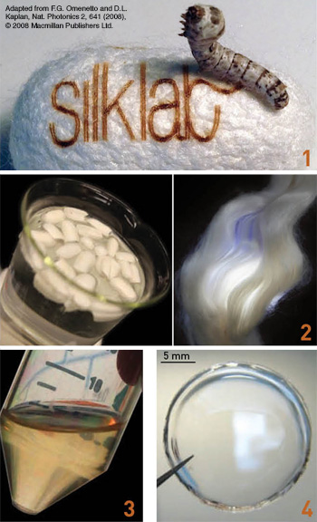 From silkworm to silk film: 1. Silkworms use the raw material in mulberry leaves to create silk fiber to spin their cocoons. 2. For use in optical devices, cocoons are cooked (left) to isolate silk fibroin fibers (right). 3. These tough fibers are dissolved to obtain liquid silk. 4. The silk solution can then be formed into multiple material formats, including clear free-standing films (shown), nanoparticles, sponges, adhesives and gels, blocks and fibers.
In addition to mechanical strength and toughness, silk fibroin has remarkable optical properties. Silk films are transparent to visible light of all wavelengths and have extremely low surface roughness (less than 5 nm rms). These properties make silk films a suitable material for a wide range of optical devices, including diffraction gratings, phase masks, white-light holograms and photonic crystal lattices—all fashioned simply by casting the fibroin-water solution onto an appropriate surface.
Processed in this way, silk is able to reproduce surface features as small as 10 nm. And silk’s optical capabilities—coupled with its advantages in biomedical applications and systems (see sidebar, “Molecular bubble wrap,” on right)—open up some surprising opportunities for new devices, sensors and treatments.
Creating silk devices
Silk films are probably the simplest and most versatile materials from which regenerated silk can be transformed. The process is simple: silk fibroin solution is cast onto a surface and allowed to dry. As the water evaporates, the silk proteins self-assemble into a transparent sheet that can be lifted free of the surface. The volume and concentration of solution controls the thickness, which can range from a few nanometers to several hundred microns.
When the liquid silk solution is cast onto a patterned substrate, the liquid will fill any crevices on that surface, so that the resulting film conforms to the shape of the mold, leaving a perfect inverse replica with high fidelity and resolution. Suitably designed masters can allow formation of a wide variety of optical devices. On the downside, the simple cast-and-dry process is relatively slow in ambient conditions; it usually takes 12 to 36 hours for the solution to fully dry. Films can also shrink while drying and can become deformed when the film is removed from the master.
As an alternative, silk films can be cast on a flat substrate and patterns can subsequently be embossed or stamped onto the dry silk film. Careful application of heat and pressure results in parts of the film returning to an almost liquid state. In this phase, the films can conform to extremely small features in the master plate. This faster technique makes it possible to rapidly produce large numbers of devices.
Master molds are commonly made from silicon wafers—but, again, these masters are expensive and slow to produce. Protein-on-protein printing, in which one silk film is used to pattern another, has emerged as an alternative, and master silk molds for this process can be quickly and inexpensively produced using several methods, among which is multiphoton laser ablation.
|
The protein sequence of silk includes small residues of the amino acid tryptophan; this, along with tyrosines, is responsible for silk’s characteristic absorption spectrum, which has peaks in the mid-ultraviolet region (270 nm). When illuminated with focused femtosecond pulses of 810 nm light, an efficient three-photon absorption process takes place at the beam focus, converting the light energy into heat and vaporizing the silk. When applied to silk films, this property allows for the rapid generation of arbitrarily shaped patterns with a resolution of around 1 µm. These patterned films can subsequently be used as masters to emboss flat silk films, reducing from weeks to only hours the time from conception of an idea to dozens of completed samples.
Nanoscale patterning requires a different method. Using electron beam writing and basic lithographic techniques perfected in the microchip industry, silicon master stamps can be produced with feature sizes on the order of 10 nm. Once formed, these masters can be used repeatedly to pattern silk films into a variety of diffractive optical elements.
As an example, aperiodic gratings are structures that diffract light in specific ways depending on the pattern of the grating, the angle of incidence and, most important, the refractive index of the surrounding media. Layers as thin as a single molecule coated on these gratings will dramatically change the far-field color pattern. When combined with silk, these gratings offer an exciting new realm of optical sensors in which the sensing element and the readout are bound together, and the entire sensor design is simplified.
Blood sensors and inverse opals
The prospects for these silk devices become compelling when they are pressed into biomedical service. For example, silk’s ability to stabilize biological systems means that micro- and nanopatterned silk can be doped with biologically relevant compounds to act as sensors. As an example of this merging of optical
form with biological function, a proof-of-concept device consisting of a free-standing silk diffraction grating containing human blood was developed by simply mixing blood with the silk aqueous solution and casting the result onto a diffractive substrate. The hemoglobin contained in the free-standing silk-blood grating maintained its ability to bind and unbind oxygen while being used as an optical element. Thus, the diffraction grating could alter its spectral response as a function of the oxygen concentration surrounding the grating—the silk-blood-grating was able to “sense itself” as a function of the surrounding environment.
While the discussion has focused thus far on 2-D optical elements, silk can also be shaped into 3-D structures and photonic crystals. These highly organized lattices have a periodicity on the order of the wavelength of light (around 400 nm); when light impinges on such a structure, the multiple reflections from each layer boundary result in destructive interference for forward-propagating light of certain wavelengths. This means that light from a certain spectral region is unable to propagate through the crystal and must be reflected.
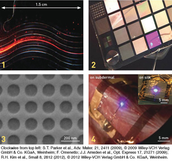 Examples of silk devices at various scales and with differing optical applications: 1. Printed silk waveguides. 2. A silk card containing diffractive optical elements (microlens arrays, phase masks, diffraction gratings). 3. An electron micrograph of a 2-D photonic lattice. 4. An InGaN thin-film LED on a silk substrate, which conforms to animal skin and is wirelessly powered—an example of biological integration of silk-hybrid photonics.
Photonic-crystal structures, though highly organized and incredibly tiny, are found in nature—such a structure, for example, accounts for the shimmering iridescence of a blue morpho butterfly wing. In addition to being beautiful to look at, these photonic crystals are very sensitive to the refractive index of the surrounding medium. In air, they might reflect a specific color as blue or green, while in water the reflectance can shift to the other end of the spectrum to appear orange or red.
With this example in mind, our group has developed an analog in silk: inverse opals. Regular opals consist of a matrix of tightly packed silica spheres—each between 150 and 300 nm in diameter, which is, not coincidentally, about half the wavelength of visible light. The difference in refractive index between the spheres and the gaps surrounding them gives rise to opals’ characteristic play of colors. And, as with many optical phenomena, the inverse structure—spheres of air, surrounded by a matrix of other material—can yield a similar result.
Silk inverse opals are made by first producing opals from poly(methyl methacrylate), or PMMA, spheres that form spontaneously in water. These direct opals can then be immersed in a silk solution which is allowed to crystallize. The PMMA spheres are then dissolved away using acetone, leaving the silk behind. As with all materials made of silk, these inverse opals can be doped with drugs, dyes or enzymes and safely implanted within the body.
Microfluidic devices
The combination of properties exhibited by silk makes it a useful and versatile platform for microfluidic sensors. These sensors work by flowing tiny volumes of liquid through very small channels. Most medical testing equipment requires several milliliters of fluid, while microfluidic sensors typically require about a thousand times less volume. This allows for more tests to be done on the same volume of sample in a smaller amount of space. Lab-on-a-chip devices are currently being produced that can replace roomfuls of equipment with a device that can be held in one hand.
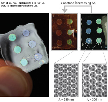 Inverse opals: (Left) Free-standing silk film with nanopatterned 3-D inverse opals, displaying iridescence according to the lattice constant (Λ) of the devices. (Top right) The devices change color when infiltrated with a fluid, thus changing the index contrast of the photonic crystal lattice. (Bottom right) Electron microscope image of the different silk inverse opals.
Silk is well suited for these sensors. Sensitive molecules can be doped into a silk film and stabilized in the device. Depending on the sample and the target to be analyzed, the response can be read colorometrically (taking advantage of the optical transparency of silk) or using an optical element such as a diffraction grating to measure spectral changes. When packaged into a microfluidic device, these sensors can be more robust and longer lasting than if they were made from more conventional materials.
Toward implantable optics
When light interacts with tissue, absorption, single-scattering and multiple-scattering processes all play a role in directing where the photons travel. Implantable optical devices have tremendous potential to guide light within the body, allowing for enhanced imaging, optogenetic stimulation or more targeted light delivery for photodynamic therapies. Silk has the optical, mechanical and biological properties necessary to excel in this role.
One example is the use of implantable silk mirrors to increase the signal of optical imaging methods. Microprism arrays (MPAs) have the ability to collect incident light from a wide angle and reflect it at a much narrower angle. These structures are found in road signs and running shoes that seem to glow when illuminated by a car’s headlights. Simply casting silk solution over an MPA master will result in a silk MPA. When implanted, these MPAs collect incident light and reflect it back. By scanning an illumination source and a detector over the skin, the precise location of the MPA can be seen by an increase in the amount of reflected light. This increase in signal could enhance optical imaging deep within the body.
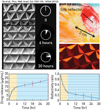 Implantable silk mirrors: (Top left) Electron microscope image of silk microprism arrays degrading in the presence of enzymes. (Top right) Silk microprism array loaded with the chemotherapeutic doxorubicin. When these silk devices are loaded with drugs in this manner, the drug is released and correspondingly the microprisms change their geometry, allowing for correlation of the reflectivity from the silk device and the amount of drug delivered (bottom).
The silk mirrors can also be doped with drugs or other compounds. As the mirrors degrade in the body, the drug will be slowly released. As the drug is released, the amount of light reflected from the mirrors will also degrade—which means that the amount of drug that has been delivered can be determined using the change in reflectance. This simple technique offers a way to monitor an injury site optically, deliver a drug where and when it’s needed and assess how well the drug is being delivered.
A new silk road for biomedicine
The integration between photonics and biology could revolutionize the way healing, surgical integration, vascular ingrowth, brain function, cancer progression or regression and many other common health issues are tracked. Even everyday health monitoring could benefit from using the physiology of the body to modulate photons and relay information to an external optical receiver. The impact of an implantable device that matches the performance of current technology and simultaneously can be an integral part of the physiological fabric is potentially immense. The option to move from outside-in monitoring to inside-out monitoring would redefine portability, bring long-term sensing directly to the site of interest and contribute to the development of personalized medicine.
Silk could help to enable just such a revolution. It is a synergistic material, and each of its characteristics—optical properties comparable to glass; strength comparable to Kevlar; biocompatibility; the abililty to design, tune and control its degradation lifetime; and the ability to stabilize drugs—is crucial to the next generation of advanced medical devices. The combination of all of these qualities in one material truly makes silk more than the sum of its parts.
Matthew B. Applegate, Mark A. Brenckle, Benedetto Marelli, Hu Tao, David L. Kaplan and Fiorenzo G. Omenetto are with the Department of Biomedical Engineering, Tufts University, Medford, Mass., U.S.A.
References and Resources
-
F.G. Omenetto and D.L. Kaplan. “A new route for silk,” Nat. Photonics 2, 641 (2008).
-
H. Tao et al. “Silk materials—a road to sustainable high technology,” Adv. Mater. 24, 2824 (2012).