

Composite illustration Alessia Kirkland/Source images Thinkstock and Apple
What determines the tipping point for new technologies in the consumer market—that is, the point at which devices go from cool-to-have to must-have for most people? It probably occurs when there is alignment between engineering breakthroughs, social trends and corporate profit motives. Camera phones are a case in point.
The first instance of a photograph being taken on a cell phone and publicly shared is said to have taken place in 1997, and it was an image of a newborn girl taken by her proud father. Today, that ability is so commonplace that any parent carrying a cell phone is likely to have instant access to a family album.
Within each smart-phone camera module lies a closely tied group of core technologies, including:
-
An image sensor small enough to fit within a very tight space but sensitive enough to
produce images of acceptable quality; -
A workable lens system for manipulating the image, which allows meaningful pictures
to be taken; -
Wafer-level optics and packaging technologies, which enable the construction and assembly of the camera modules in manufacturing processes compatible with semiconductor mass production; and
-
In many modern camera phones, a flash unit that provides additional illumination and improves the image quality; this is usually in the form of an LED.
Camera phone development has been driven by more than pure engineering; the pull of consumer behavior and the push of software development have been at least as significant. The impact of Apple and the iPhone cannot be underestimated, since many consumers have come to understand and embrace mobile imaging through their iPhones.
According to analysts at the market intelligence firm IDC, cell phones and handheld cameras became linked technologies as a result of the widespread adoption of mobile apps and the resulting consumer demand for the capacity to capture and share images directly from one’s phone (through Facebook and email, for example).
But optics remains the key for making it all possible. Picture quality has been improved through more responsive sensors and lenses, while designers of mobile devices have constantly pushed engineers towards ever-tinier technology. The difficulties involved in fitting effective camera technology into a mobile handset remain the potential Achilles heel of such devices, at least when compared to digital single-lens reflex and digital still cameras. However, the methods used by engineers and vendors to square that circle have led to some true innovation in the market.
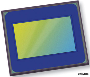 OmniVision’s latest sensor, the OV5680, is targeted at camera phone applications. It uses the company’s backside illumination technology.
Courtesy of Omnivision
Image sensors
The image sensor market is always driven towards tinier, lower-cost devices with smaller pixels, higher resolution and better image quality. Companies currently meet those demands through complementary metal-oxide-semiconductor (CMOS) technology.
Developments in this area have allowed for a steady stream of improvements in CMOS-based image sensors, and that has enabled these devices to be miniaturized and incorporated economically into the road maps of camera phone vendors while still delivering acceptable image quality. Compared to older charge-coupled device-based systems, CMOS-based cameras consume significantly less power, offer higher levels of integration with assemblers’ work flows and contribute to lower overall system costs.
Current-generation sensors from the California-based developer OmniVision use a design known as backside illumination (BSI), which is intended to squeeze the maximum performance from the sensor without affecting its suitability for a mobile environment.
The manufacture of a conventional CMOS sensor starts by placing the core photodiode of each pixel onto its silicon wafer, and then depositing above it the layers of metal circuitry needed to connect the pixels and their associated circuitry together. The necessary lens and filter components then sit on top of that. Unfortunately, once the process is complete, a great deal of material lies between the lens at the top and the photodiode at the bottom, inhibiting the sensor’s sensitivity and performance.
BSI attacks this problem by flipping the wafer over once the metal circuitry is in place, and attaching the lens and filters to the backside instead, allowing light to enter the sensor at a point much closer to the photodiode itself. This approach has its own challenges, not least of which is the need to grind the reverse side of the silicon wafer down to a carefully controlled thickness before attaching the lens and filters. But the rewards are higher sensitivities and the ability to pack more pixels into the available space.
Sensors with BSI are currently very big news in smart phone circles. The iPhone 4 has a 1.75-µm-pixel BSI sensor, while the HTC EVO 4G has a 1.4-µm-pixel sensor. In both cases, the sensors are manufactured by OmniVision.
Analysts at the market research firm iSuppli predict that shipments of BSI sensors for mid- to high-end smart handsets will rise to 300 million units by 2014—up from 33.4 million in 2010 and virtually zero the year before that. Seventy-five percent of such mobile devices will feature BSI sensors by then.
|
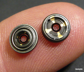 Liquid lenses developed by Varioptic can help mobile devices to demonstrate sophisticated image processing capabilities. Optilux, an independent U.S. company, is now developing the technology for mobile applications.
Courtesy of Varioptic
Liquid lenses and image processing
The idea of a lens whose active medium is a liquid rather than a solid is nothing new, but it has found a fresh potential application in the era of mobile devices. Rather than presenting a set of fixed and unchanging optical properties, liquid lenses can be reshaped in situ, altering the path of the light traveling through the lens.
The liquid lenses originally developed for mobile devices by French vendor Varioptic use the principle of electrowetting, in which a small applied voltage brings about a change in the contact angle of a fluid on a planar surface.
The heart of a liquid lens features a watertight cell containing two transparent, optically perfect but nonmiscible liquids. Applying a voltage induces the electrowetting effect and causes the curvature of the interface between the liquids to change, effectively pulling the lens into a different optical configuration and changing its power.
This change can take effect very rapidly, requiring only some tens of milliseconds, and it is reversible with little or no hysteresis. The phase shifts that are achievable can nonetheless be substantial, potentially equating to 40 diopters over a 3-mm aperture.
Liquid lenses offer a route to effective auto-focus capability within the form-factor requirements of a phone handset. They also allow for an image to be manipulated in ways that solid lenses cannot achieve without difficulty. Incorporating multiple electrodes into the structure allows for the judicious application of various voltages at different points, bringing very fine control over the shape adopted by the lens. Four carefully placed electrodes allow both the radius and tilt of the lens to be controlled. An eight-electrode configuration can successfully configure for sphere, tilt and cylinder corrections. These adjustments can be made in real time.
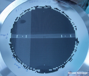 A wafer of lens assemblies. Wafer-level optics involves building as much of the optical train as possible at the wafer level, prior to dicing.
Courtesy of Nemotek Technologie
While liquid lens technology has not yet been integrated into mainstream mobile phones, it has attracted real commercial interest. For example, Optilux, a California-based company that recently acquired the exclusive rights to develop Varioptic’s lens technology for smart phones and tablets, has demonstrated an optical image stabilization (OIS) technique that addresses the inevitable camera shake that all handheld devices are prone to.
The OIS module monitors user-induced vibration through a motion sensor and translates that into a voltage, after which a processor determines where best to apply it to a liquid lens via a four-electrode configuration. The result is a system that is able to adjust the focus and tilt in both x and y directions, responding to camera movement in real time and steadying the output image.
Wafer-level optics
It has long been clear that there are economic advantages associated with assembling multiple camera modules at the wafer scale and then dicing that wafer to produce a large number of complete camera assemblies. One significant reason is that this approach allows for a better synergy with semiconductor manufacturing processes.
But there are complications. Camera modules may contain more than a dozen components, including lenses, filters, spacers and autofocus mechanisms, and carrying out every required manufacturing stage on a semiconductor wafer is not practical.
 A single-element VGA lens from Tessera. Wafer-level technology platforms developed by Tessera are operated by several licensees, although Tessera itself has withdrawn from wafer-level optics.
Courtesy of Tessera
A more realistic goal, as defined by specialist developers Tessera, in Calif., U.S.A., is to produce wafer-level cameras by making the optical train at the wafer level, dicing it into individual optical stacks, and then carrying out die-to-wafer assembly to build camera modules.
In order to turn the approach into a viable and commercial manufacturing technique, developers have had to come up with new ways to get the most out of their assembly equipment, as well as to make advances in the makeup of the optical elements being assembled.
A key part of the value proposition of the wafer-level camera is not just that the camera module is cheaper, but that it should be reflow compatible, allowing it to be mounted onto the main printed circuit board along with the other surface mount components. The hope of assemblers is that novel lenses and other new optical technologies can then be more easily incorporated into modules, presenting an obvious cost advantage.
Analysts forecast that reflowable wafer-level cameras will account for more than 30 percent of the camera modules manufactured annually by 2013.
|
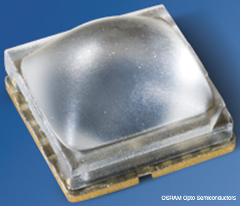 The Oslux LED is designed specifically for mobile applications, through an optimized chip and lens design that results in greater brightness. The lack of flash illumination was a serious handicap for early camera phones and a cause of much frustration for consumers.
Courtesy of OSRAM Opto Semiconductors
LED flashes
A major constraint of the first smart phone cameras was the absence of any in situ flash illumination incorporated into the handset. With low-light performance always acknowledged to be a weak spot, the arrival of an LED flash to the iPhone platform with the iPhone 4 in 2010 significantly boosted that device’s popularity.
Since then, several parallel advances in LED technology have increased their suitability for use in mobile devices. Their small dimensions, high mechanical stability and longer lifetimes compared to flash tubes based on xenon or krypton are all attractive features. They also require lower voltages than conventional units in order to create a flash, and they can usually do so with negligible charging time. If needed, they can easily provide longer flash durations or even continuous illumination.
Now that many modern smart phones can record video, LEDs have also proven to be well suited for use as flash lamps for video cameras. In this case, the significant advantage is that the light flashes can be synchronized to the video frames, so that the flash only activates during frame capture and is turned off between frames. This reduces the energy usage considerably.
The illumination characteristics of LEDs in mobile devices are rather different from those shown by gas tubes. Conventional non-LED flash units typically illuminate a subject with more than 1,000 lx, in a flash lasting from 15 µs to 2 ms, depending on the coverage range. Two consecutive flashes can be anything from one to five seconds apart, mainly due to the need to recharge the capacitor between fires. The color temperature of the flash is nominally between 5,500 and 6,000 K.
In mobile phones, the parameters are rather different, since the minimal illuminance required depends on the optical resolution of the camera chip being used. Higher resolution sensors require more illuminance because the illuminance that bounces back from the scene must be spread out over the pixels in the sensor; thus, if there are more pixels present, then more total illuminance must be supplied to the scene in order to give each pixel enough of a “share” to produce a quality image.
In a basic camera phone, the resolution can be 3 to 5 mega-pixels, requiring in turn that the minimal center illuminance at a distance of 1 m from an attached LED flash falls between 80 and 200 lx, according to figures from Osram Opto Semiconductors, which has developed two LED flash products designed for mobile devices. At the higher end of available resolutions, the light requirements are even tougher: A sensor of 8 megapixels or above needs at least 300 lx illuminance.
Although LEDs are available in a variety of colors and could be used as flash units, only white LEDs are currently used. These typically employ the principle of color addition, taking a primary blue output from a blue semiconductor chip and then using a yellow converter to supply the appropriate complementary color to produce a white output. The advantage of this is that it ensures that the color temperature is effectively specified when the LED is manufactured, since the color mixture is defined and fixed. In Osram white LEDs, the color temperature falls in the range of 5,000 to 7,000 K.
Seeing the future
Optical technologies that are currently under development could eventually have a significant impact on the camera phone market for vendors and consumers.
One tantalizing prospect is the arrival of microlens arrays that mimic the composite eye structures found in insects. Replacing the single lens or multiple lens assemblies used in camera modules with a single microlens array could allow the entire module to become considerably thinner, and avoid the risk of incorrect alignment among multiple optical elements—a situation that manufacturers must constantly guard against.
Andreas Tünnermann of the Fraunhofer Institute for Applied Optics and Precision Engineering in Jena, Germany, believes that a microlens array could allow an objective lens of just 1 mm thickness to be manufactured, once the arrays are successfully incorporated into existing wafer-level manufacturing processes. Consumers might then benefit from camera modules that are able to capture a wider field of view in each image.
Microlens arrays also play a part in the technology under development by two companies—which could allow consumers to make changes to photographs that they have already taken. Both the Stanford University startup Lytro and the German company Raytrix aim to breathe fresh life into plenoptic cameras, a design that is more than a century old.
Plenoptic cameras can capture the entire light field of a scene instead of the two-dimensional slice captured in a conventional image, using a microlens/photosensor array to do so. In theory, this can enable the pixels of the array to capture an image at all focal lengths—even out to infinity.
For consumers, this opens up the intriguing possibility of being able to adjust the focus of a photograph after it has been taken—to shift the focus from the foreground to the background of an existing image, for example. There is, however, one inevitable penalty: a loss of overall image sharpness, since pixels from multiple points of view must then be stored on an image sensor.
Raytrix already markets a plenoptic camera for scientific and industrial users; it integrates an array of four different types of microlenses with individual focal lengths. The company says that this enables not just the ability for software-assisted refocusing, but also a six-fold improvement in the depth of field.
Plenoptic technology currently carries a hefty price tag, with the Raytrix R5 camera starting at a basic price of €3,000 even without the addition of the extra components and software needed to handle the refocusing ability. Lytro is aiming to release its camera in 2012 at a rather more consumer-friendly price point than that.
If this and related technology is commercialized at the right price, it may mark a fundamental change in the manner in which people interact with their photos—and perhaps trigger a new technological tipping point.
Tim Hayes is a freelance writer based in the United Kingdom who specializes in optics and photonics.