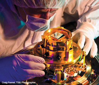
 Tom Sprafke, senior scientist at Teledyne Imaging Sensors, prepares the James Webb Space Telescope’s fine guidance sensor for cryogenic performance testing.
The improved performance of FPAs was made possible by technological advances in four areas: detector material growth and processing; readout circuit design; large FPA hybridization; and packaging. This article provides a synopsis of the technology of today’s infrared FPAs and the performance that a systems engineer should expect when specifying an infrared FPA.
The arrays continue to grow in size, with 16 megapixel infrared imagers becoming widely used and FPAs with hundreds of millions of pixels under development. We concentrate on the highest performance infrared (IR) arrays that are made from HgCdTe detector material. These arrays are used for the most demanding applications, such as the Hubble Space Telescope, the James Webb Space Telescope and planetary science.
Hybrid CMOS FPA technology
The most advanced IR arrays are made with a hybrid complementary metal-oxide-semiconductor (CMOS) architecture, which combines the best qualities of IR detector material with the performance achieved by advanced CMOS integrated circuits. In this architecture, the first three steps of digital imaging (as listed in the table below) occur within the detector layer, which detects the light and collects photocharge into pixels, using electric fields created by a p-n junction within each pixel.
The detector material can be fabricated as either p-on-n, which is a p-type implant into n-type bulk, or vice versa, n-on-p. (In p-on-n detectors, the p-n junctions collect holes, and in n-on-p detectors, the p-n junctions collect electrons.) The p-n junction in each pixel is connected to the read-out integrated circuit (ROIC) by an indium interconnect, one indium bump per pixel. The CMOS readout circuit converts charge to voltage and multiplexes the voltage signal from each pixel to the edge of the array.
The output from the array can be an analog signal or a digital signal if the ROIC includes an analog-to-digital converter. Whether the junction collects holes or electrons, all performance quantities, such as full well and readout noise, are stated in units of electrons.
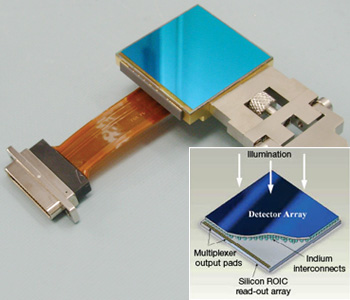 Hybrid CMOS FPA architecture used for the highest performance IR arrays. The hybrid is a combination of a detector layer and a CMOS read-out integrated circuit (see inset). Shown here with handling tool is a 2,048 × 2,048 pixel (18 µm pixel pitch) H2RG array that is widely used in astronomy.
The highest performance IR detector material
The best detectors are crystal lattices that provide well-defined separation between the valence band, within which electrons are captive, and the conduction band, where electrons are free to move through the crystal lattice. The energy separation between the valence and conduction bands is called the bandgap of the material; this bandgap determines the wavelength range detectable by the detector material. If a photon with energy greater than the bandgap is absorbed, an electron will be excited from the valence band and placed into the conduction band. The photocharge in the conduction band can be collected into pixels and measured.
A unique type of infrared detector material is mercury-cadmium-telluride (HgCdTe, referred to as “mer-cad-tel,” or “MCT”). What makes HgCdTe special is the fact that its bandgap—which depends on the mixture of mercury and cadmium—can be tuned by more than an order of magnitude, from less than 0.1 eV to greater than 1 eV.
A more exact expression of this ternary compound is Hg1–xCdxTe, for which 50 percent of the atoms are tellurium, and the remaining half are composed of a mixture of mercury and cadmium (when x=1, HgCdTe reduces to CdTe). The longest wavelength of light that can be sensed by a detector is inversely proportional to the bandgap; HgCdTe is routinely grown with cutoff wavelengths that range from 1.7 to 16.5 µm.
The growth method that produces the highest performance HgCdTe material is molecular beam epitaxy (MBE). An MBE system grows the HgCdTe layer at a high vacuum, starting with a CdZnTe substrate that has a lattice spacing that closely matches HgCdTe. The MBE system evaporates and deposits Hg, Cd and Te onto the substrate. The rate of deposition is slow, building an atomic layer every 1 to 2 s, and it takes 4 to 6 hours to grow an HgCdTe detector layer. With MBE, the mixtures of Hg, Cd and Te, and additional dopants, can be precisely controlled. This “bandgap engineering” enables MBE to grow complicated structures in the HgCdTe layer that provide the highest level of performance.
|
The six steps of digital IR imaging
|
|||
| Digital imaging step | Technologies | ||
| 1 | Get light into the detector |
Anti-reflection coating Substrate removal |
Infrared detector material |
| 2 | Charge generation | Detector material growth | |
| 3 | Charge collection | p-n junctions | |
| 4 |
Charge-to-voltage conversion |
Amplifiers optimized for flux, speed and noise • Source follower • Capacitive Transimpedance Amplifier • Direct Injection |
CMOS inegrated circuit |
| 5 | Signal transfer |
Multiplexer Scanner |
|
| 6 | Digitization | Analog-to-digital converters | |
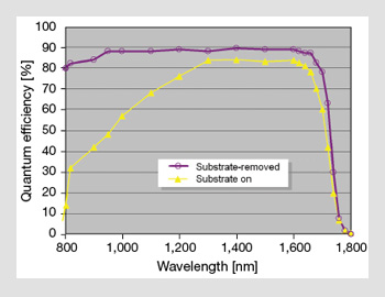 The quantum efficiency of 1.7 µm HgCdTe detector material shown for two cases: CdZnTe substrate on the FPA and with the CdZnTe substrate removed.
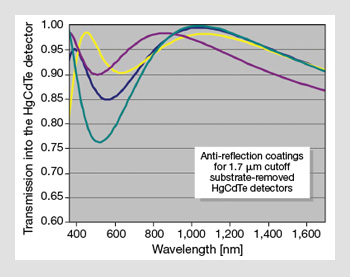
The AR coating can be optimized for peak quantum efficiency over the infrared region (0.9-1.7 µm), as shown in the green and blue curves, or optimized for the visible-infrared band (0.4-1.7 µm), demonstrated by the yellow curve. AR coatings can be similarly optimized for other wavelength regions.
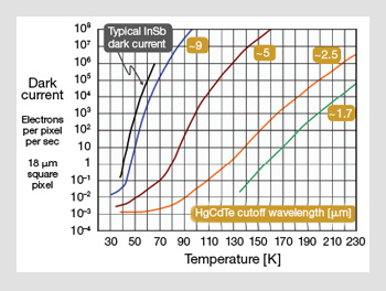
The dark current of MBE grown HgCdTe detector material is shown for an 18-µm pixel and can be scaled for pixel pitch. Only approximate cutoff wavelengths are shown, since cutoff wavelength is a function of operating temperature.
The performance of HgCdTe is defined primarily by two parameters—quantum efficiency (QE) and dark current. The figure at the top right presents two QE curves, one with the CdZnTe substrate included, and one with the CdZnTe substrate removed after hybridization.
Removing the substrate has several benefits. For example, it increases quantum efficiency in the short-wave infrared from 1 to 1.5 µm and provides sensitivity to visible light, down to 400 nm, since the CdZnTe substrate absorbs light for wavelengths shorter than 800 nm. It also eliminates the fluorescence caused by the absorption of cosmic rays in the CdZnTe. After the substrate is removed, an appropriate anti-reflection (AR) coating is applied. Without an AR coating, about one-third of the incident light would be reflected at the first surface and would therefore go undetected.
Dark current is the flow of charge across the p-n junction in the absence of light. Since it is not possible to distinguish dark current from photocharge and, like the photocharge itself, dark current has a Poisson noise distribution, very low dark current is required for sensing low flux illumination. Detector materials made by the MBE process achieve the lowest dark current of all HgCdTe detectors. Dark current is a function of area, temperature and cutoff wavelength.
The bottom figure on the right presents dark current for MBE-grown HgCdTe, scaled for an 18 µm square pixel. The benefits of low dark current are twofold. First, low dark current enables the most sensitive flux measurements to be made at very cold temperatures. Secondly, low dark current enables operation at the highest temperature for a given level of performance, thereby decreasing thermal load on the instrument cooling system.
Readout integrated circuits
After the photocharge has been collected into pixels, the charge flows to the ROIC via the indium bump bond. A key aspect of the hybrid CMOS imager architecture is that the ROIC is fabricated with the same equipment that is used for making high performance integrated circuits (ICs, or computer chips). With the highly advanced tools used for IC design, the functionality of the ROIC is limited only by the imagination of the designer and the space constraints of the pixel.
Furthermore, space constraints can be overcome by using finer design rules (which denote the smallest feature that can be made on the ROIC), and ROICs are routinely made in 0.25, 0.18 and 0.12 µm design rules. The most basic functionality of the pixel is charge-to-voltage conversion, and there are three basic types of amplifiers that can perform this function. However, it is possible to include signal processing within the pixel, such as range detection or background subtraction, and some complex pixel designs have incorporated nearly 700 transistors within a pixel.
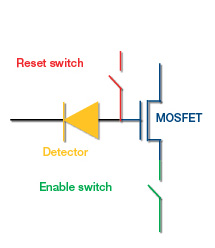
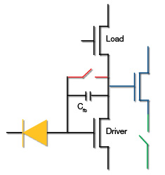
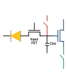
The two imaging parameters that are the most significant drivers for ROIC pixel design are the expected flux of the illumination and the readout rate of the FPA. These two parameters define the full well of the pixel (i.e., how much charge must be stored in one integration period) and the noise level of the amplifier required for photon noise-limited performance. There are three basic types of amplifiers used in CMOS ROIC pixels, as shown in the figure on the right. These amplifiers provide a range of full well and readout noise performance that can be optimized for a specific application.
After charge-to-voltage conversion, the ROIC multiplexes the voltage signal to the edge of the FPA, where it can be read out to off-chip electronics. The multiplexer can be designed to read out the entire array, read out windows of the array, or to subsample the pixels (e.g., every other pixel and every other row), or to perform almost any other imaginable mode of operation. At the system level, it is critical to clearly define the complete concept of operations of the instrument, and the FPA at the beginning of a development program. An operation mode that is relatively easy to implement at the initial design stages can become very hard, if not impossible, to implement at an advanced stage of development.
The last step in digital imaging is the conversion of the analog voltage to a digital value. For imaging sensors, analog-to-digital converters (ADCs) are typically provided in the following resolutions and conversion rates: 12 bit / 40 MHz, 14 bit / 20 MHz, 16 bit / 500 kHz. The power of ADCs continues to drop so that ADCs can now be integrated into the ROIC without significant additional heat load. For the highest performance ADCs, the power expended is 1 to 2 mW per MHz for a 12-bit ADC, 3-4 mW per MHz for a 14-bit ADC, and 3 mW per 100 kHz for a 16-bit ADC.
|
Types of amplifiers used in hybrid CMOS IR FPAs
|
||
|
|
|
|
|
Source Follower (SF)
|
Capacitive Transimpedance Amplifier (CTIA)
|
Direct Injection (DI)
|
|
• Integration on detector node • Low power and compact (3 FETs/pixel) • Ideal for small pixels and low flux • Poor performance for high flux • Full well: ~100,000 electrons • Readout noise: <15 e– |
• Versatile circuit suitable for all backgrounds and detectors • High linearity • High power, higher noise and larger circuit than SF for low flux • Worse performance than DI for high flux • Full well: ~1 million electrons • Readout noise: <50 e– |
• Extremely small circuit • Large integration density in pixel • High well capacity for high flux applications • Ultra low power • Poor injection efficiency for low flux applications • Full well: 10s of millions of e– • Readout noise: <1,000 e– |
Readout noise is a fundamental, although undesirable, attribute of the charge-to-voltage conversion process, but reset noise is a greater noise source if not corrected. A method called correlated double sampling (CDS) removes reset noise. Readout noise, as stated here, takes into account the CDS method.
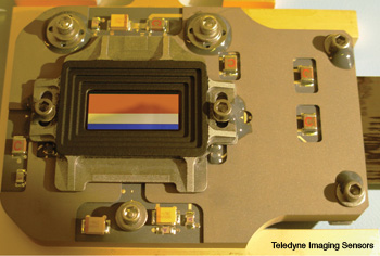 The lightweight focal plane assembly used in JPL/NASA’s Moon Mineralogy Mapper. The package incorporates a Teledyne TCM6604A 640×480 pixel, 3.5 µm IR array with a three zone order sorting filter. The FPA is substrate-removed so that a 0.4-3.5 µm bandpass is sampled by the spectrograph.
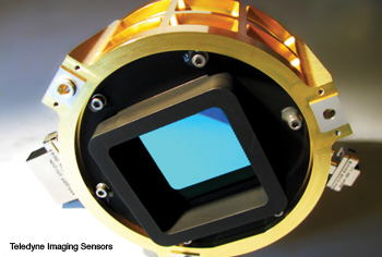
Fine guidance sensor of the James Webb Space Telescope.
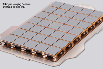
Large IR mosaic prototype array with 35 H2RG arrays. The array has a total of nearly 147 million pixels. Each of the H2RG arrays has 2,048×2,048 pixels.
Packaging FPAs
The packaging of an infrared FPA provides the mechanical, thermal and electrical interface to the instrument. Often, the system-level requirements are very strict, with mechanical alignment of the array to within a fraction of a pixel and minimal thermal load on the spacecraft. In nearly every space mission, reduction of mass is a driving requirement.
An example of a lightweight package that meets fine alignment requirements is the multilayer ceramic structure used in the Moon Mineralogy Mapper, an instrument developed by the Jet Propulsion Laboratory. It will be launched in mid-2008 on India’s first mission to the Moon, Chandrayaan-1. Using the monolithic ceramic package approach, engineers produced a focal plane assembly that weighs less than 60 g. By integrating the electrical circuitry into multiple layers of the ceramic motherboard, they minimized the package size and weight.
Each material in the system was specifically selected to match the coefficient of thermal expansion of adjacent parts of the system. Thus, the thermal stresses and differential motion between the parts of the system were minimized and, most important, the spatial relationships between the detector, filter and the interface mounting points were maintained to within a few micrometers. The order sorting filter is mounted 50 µm above the detector surface—half the width of a human hair—to minimize blurring from the filter.
A key aspect of FPA packaging is thermal management. One example is the fine guidance sensor (FGS) used on the James Webb Space Telescope (JWST) to provide optical pointing stability. Developed with the financial support of the Canadian Space Agency, the FGS package was designed to simultaneously meet several requirements:
• To provide enough rigidity to survive the launch,
• To provide enough compliance to prevent breakage during cool down to 20 K, and
• To provide thermal isolation and highly stable temperature of the imaging array.
Finite-element analysis was used to optimize the design and predict the mechanical and thermal performance. During vibration tests, the resonance frequency matched the predicted performance to within 5 percent, and the thermal design specifications have also been demonstrated in practice. The temperature of the imaging array can be stabilized to 1 mK while the temperature of the cold thermal strap to the FPA varies by as much at 5 K. The FGS package is now rated as NASA Technology Readiness Level 6 (TRL-6).
For mechanical interface between the focal plane assembly and the instrument, the trend in industry is to provide packaging that enables rapid mechanical assembly without laborious optical alignment. To enable this level of integration, the package design must include kinematic mounts that have highly accurate mounting points. This approach provides interchangeable solutions that minimize the laborious optical alignment process at the system level, and allows the system integration team the possibility of rapidly switching focal plane assemblies as required.
Many astronomy programs have proposed conducting large surveys that will measure more than 100 million galaxies or stars. Scientists must make a large number of measurements to gain the statistical information required for mapping the dark matter and dark energy in the universe and finding planets around other stars. While the size of individual sensor chip assemblies continues to grow—4096 × 4096 pixels have been demonstrated in a single hybrid—the very large FPAs required for many space missions will only be achieved by making a mosaic out of a large number of individual arrays.
Over the past decade, infrared FPAs have reached an extremely high level of quality. Their performance is outstanding, with 90 percent quantum efficiency, low readout noise and low dark current. In addition, the readout circuits provide a great range of functionality, and the packaging technology has enabled very large mosaics to be assembled into focal plane arrays with hundreds of millions of pixels. Extremely high-performance IR focal plane arrays will play an integral role in driving space science into the future.
[ Thomas Sprafke and James W. Beletic are with Teledyne Imaging Sensors in Camarillo, Calif., U.S.A. ]

