
Scatterings
Lab-on-a-Chip Integrates Microfluidics, Optical Traps
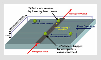
In a new type of “lab-on-a-chip” technology, particles in a microfluidic system are sorted by light.
 Numerical simulation of the Cornell group’s trapping experiment. The optical waveguide propulsion is perpendicular to the direction of the pressure-driven flow in the channel.
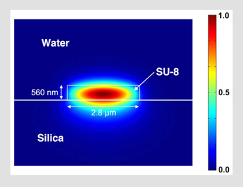
Electric field profile of the quasi-transverse-magnetic mode for a water-clad SU-8 waveguide on a fused silica substrate. The waveguide’s height and width are 560 nm and 2.8 µm, respectively.
In a new type of “lab-on-a-chip” technology, particles in a microfluidic system are sorted by light. Optical transport adds another method of controlling movement through these tiny devices beyond pressure-driven flow.
…Log in or become a member to view the full text of this article.
This article may be available for purchase via the search at Optica Publishing Group.
Optica Members get the full text of Optics & Photonics News, plus a variety of other member benefits.