
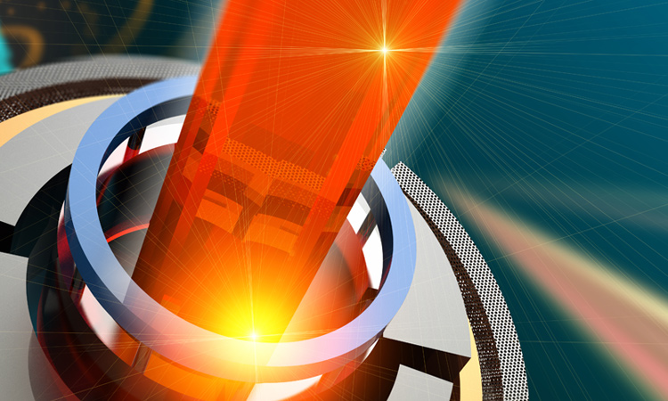
 [Getty Images]
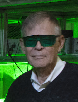
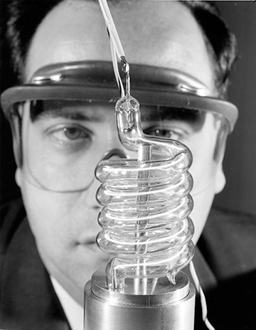 Theodore Maiman, in a May 1960 photograph from Hughes Research Laboratories. [Courtesy of HRL Laboratories, LLC]
Over the years, the photo has become an icon of engineering and scientific discovery. A youthful Theodore Maiman, slightly out of focus and clad in safety goggles, stares intently at the laser apparatus standing out sharply in the foreground—a slender ruby rod, surrounded by the coiled photographic flashlamp that served as the laser’s optical pump.
The publicity photo from Hughes Research Laboratories, USA, was taken to herald Maiman’s demonstration of the first working laser on 16 May 1960. The ruby rod and flashlamp shown in the picture—as author Jeff Hecht notes in Beam, his classic account of the race to create the laser—weren’t the ones that Maiman had actually used, and were selected by the photographer for artistic effect rather than scientific accuracy. But that scarcely mattered. The laser was born, and the world never looked back.
The subsequent six decades have been a riot of discovery, driving Maiman’s initial invention in undreamed-of directions. For a present-day reading on a few of those, OPN talked with eight OSA Fellows about work they’re doing now to take lasers to new wavelengths, shorter pulse durations, smaller dimensions and new applications. Here we can offer only a few snapshots from the vast frontiers of laser technology. But we hope that the resulting collage gives a hint of how far the laser has come since that first demonstration—with no sign of slowing down.
Terahertz lasers: Minding the gap
The red pulses that shot out of Maiman’s laser 60 years ago had a wavelength of 694.3 nm—the value for the R1 electronic transition of the pink ruby he used as the device’s active medium. Announcements rapidly followed of lasers using other gain media (and, hence, sporting other wavelengths): solid-state lasers, gas lasers, dye lasers, semiconductor lasers and more. Diode-pumped solid-state lasers and optoelectronic and nonlinear wavelength-conversion techniques further filled in spaces in the spectrum.
Even so, a few interesting wavelength bands have stubbornly resisted the development of cost-effective lasers. One of those is the terahertz (THz) band—sometimes called the far-infrared, and loosely defined as covering wavelengths from 30 to 1000 µm. THz radiation, being non-ionizing, is harmless to biological tissues, yet can potentially penetrate a variety of otherwise opaque substances. Thus, in addition to uses in radio astronomy, THz shows up in airport security and laboratory spectroscopy. But researchers have also envisioned a plethora of new applications in high-bandwidth wireless communications and high-resolution bioimaging—given the right light sources.
And there’s the rub. Because, while THz lasers exist, they have often been large, operated only in pulsed mode, sported limited tunability, or needed frigid cryogenic temperatures. The lack of a convenient, compact, continuous-wave laser source between the microwave and infrared bands has even been referred to as the “terahertz gap.” And, in recent years, scientists have put a great deal of ingenuity into filling it.
At center stage in that effort has been the quantum cascade laser (QCL), first demonstrated in 1994 by a team at Bell Laboratories led by Jérôme Faist and Federico Capasso. These semiconductor lasers have proved an invaluable light source in the mid-infrared “molecular fingerprint” region, and tunable mid-IR QCLs are now workhorses in compact devices for atmospheric sensing, standoff detection of explosives and other applications. Terahertz QCLs are likewise compact—but still require operation at well below room temperature, and so far have been tunable across only a limited frequency range.
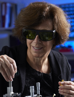
 OSA Fellow Federico Capasso co-led a team that used a mid-IR quantum cascade laser as a pump to create a tunable, room-temperature terahertz laser. [Arman Amirzhan, Harvard SEAS]
[Federico Capasso]“I hope that we can do in the far-infrared now, what we did in the mid-infrared with quantum cascade lasers.”
—OSA Fellow Federico Capasso
QCL co-inventor Capasso, now at Harvard University, USA, has been working with colleagues at Harvard, MIT and the U.S. Army on a different approach: using the QCL not as a primary THz laser, but as a pump for a molecular gas laser. These lasers, Capasso explains, use a collection of gas molecules with a permanent dipole moment as the gain medium; the right pump laser can kick those molecules to a higher-energy rotational state, and as they relax into a lower-energy state they release photons at the difference frequency between the states.
Terahertz molecular gas lasers had been created in the 1970s, but they were far from compact, with meters-long cavities. In 1986, a theoretical model by Henry Everitt, then at Duke University, USA, suggested that a much more compact version might be built. But, says Capasso, the CO2 lasers used as pumps at the time were bulky, had limited tunability and could access only a few rotational states. The idea of using mid-infrared QCLs as pumps didn’t come until much later; such a laser was reported in 2016 by researchers in France.
In 2017, Capasso and Everitt decided to team up to develop a broadly tunable THz gas laser. Two years later, in November 2019, Capasso’s team unveiled just such a device, which uses a commercial, widely tunable mid-infrared QCL to pump a 15-cm-long, 5-mm-diameter copper tube of nitrous oxide, or “laughing gas.” The device lased at room-temperature—with the lasing frequency tunable from 250 GHz to around 1 THz by tuning the mid-IR QCL pump. And, Capasso adds, the tunability should be extendable to 2 THz by using different molecular gases with different rotational states.
What will these tunable THz lasers be good for? One application, Capasso says, could be use as compact local oscillators for heterodyne detection of THz signals from space, which at present requires complex chains of frequency multipliers. There are also prospects for kilometer-range free-space communication, and, of course, much-discussed applications in security, given THz radiation’s well-known ability to pass through fabric, plastic wrapping and paper. “It really opens up a new area,” Capasso says. “I hope that we can do in the far-infrared now, what we did in the mid-infrared with quantum cascade lasers.”
Toward tabletop XFELs
Elsewhere on the frequency spectrum, Robert L. Byer of Stanford University, USA—who published his first paper on lasers only a few years after Maiman’s successful demo, and who has been associated with many laser breakthroughs ever since—has his eye on coherent X-ray sources.
“It’s overwhelming how many applications there are in the X-ray spectral range,” says Byer, “whole new ways to explore chemistry, biology, physics.” Synchrotron light sources, which churn out streams of incoherent X-rays, have already opened up many such horizons. But pushing into time-resolved studies of atomic physics and molecular chemistry requires coherent X-rays.
Several such coherent sources, X-ray free-electron lasers (XFELs), have come online in the past several decades. Byer’s Stanford office lies only around a 10-minute drive from one of them, the SLAC National Accelerator Laboratory’s Linac Coherent Light Source (LCLS), which began hard-X-ray lasing just over 10 years ago. LCLS and other XFELs, such as the European XFEL in Germany, are massive instruments; they involve kilometers-long linear accelerators and huge magnetic “undulators” to create coherent X-rays from wavelike motions of relativistically accelerated electron bunches. And, says Byer, the half-dozen or so XFELs worldwide at such mammoth facilities are “oversubscribed by a lot.”
 OSA Fellow Robert Byer is co-leading ACHIP, a project that aims to leverage laser technology to reduce the size and cost of particle accelerators, such as those at the Linac Coherent Light Source, to the scale of a chip. [ACHIP program; SLAC Linear Accelerator Laboratory/Christopher Smith]
[Misha Bruk Photography]“It’s overwhelming how many applications there are in the X-ray spectral range—whole new ways to explore chemistry, biology, physics.”
—OSA Fellow Robert Byer
Byer and the roughly 75 collaborators in the Accelerator on a Chip (ACHIP) program, which he co-leads with Peter Hommelhoff of Friedrich Alexander University Erlangen, Germany, hope to ease that capacity crunch by radically shrinking XFELs—potentially to the scale of a lab tabletop. And, as the name implies, the program would accomplish that by downsizing the required particle accelerators to chip scale—using solid-state lasers, rather than huge RF klystrons, to do the heavy lifting.
Byer says that using lasers to accelerate electrons was conceived “back in 1974,” but did not get off the ground until decades later. The DARPA-funded first phase culminated, in November 2013, in landmark papers demonstrating electron acceleration by lasers within dielectric microstructures. At that point DARPA lost interest—but fortunately, the Gordon and Betty Moore Foundation later picked up the project, rechristened ACHIP. “They wanted to fund high-risk, high-payoff research,” Byer says. “We explained that accelerator research is really high risk, and they funded us.”
At the end of 2019, the international ACHIP collaboration produced four high-profile papers in a single week, including back-to-back reports in Physical Review Letters demonstrating laser acceleration of bunched electrons with pulse durations in the range of 250 attoseconds (1 attosecond equals 10–18 seconds). Such chip-based electron accelerators would constitute only the front end of a tabletop XFEL; realizing such a device will also require the design of additional acceleration stages and a compact, laser-driven undulator to replace the magnetically driven behemoths in current XFELs—projects on which the laser community is also hard at work.
As that work comes to fruition, though, Byer believes it could spawn a new generation of compact XFELs. “Since everything is small and has a high repetition rate, we can put a resonator around the X-ray source, and build a synchronously pumped X-ray laser on a tabletop that’s both spatially and spectrally coherent,” he says.
“We think this will democratize accelerators,” says Byer. “It’ll make them small enough and cheap enough that you can design them directly to meet your science need or your manufacturing need.”
The few-cycle frontier
As Byer suggests, a key aim of the ACHIP research is to produce pulses that can probe the attosecond timescales of chemical reactions. “At the speed of light, one attosecond is equivalent to light traveling across a hydrogen molecule,” Byer notes. “That’s how short the pulses are.” It’s also 15 orders of magnitude faster than the millisecond-width pulses that issued from Maiman’s original laser.
[European Patent Office/Heinz Troll]“If you push the performance of a laser into a regime where it has never been before, something new always pops up.”
—OSA Fellow Ursula Keller
Ursula Keller has spent some three professional decades probing such mind-bendingly short intervals, first at Bell Laboratories, USA, in the late 1980s, and, since 1993, in her current role as a professor at ETH Zurich, Switzerland. In that time she’s seen, and helped realize, enormous progress in the ultrafast lasers at the heart of the work.
“In the 1970s, everything was done with dye lasers—that was the frontier,” says Keller. “You had to babysit the laser for the whole day, and at the end you could do an experiment. Now, with solid-state technology, we have much more reliable ultrafast lasers at many wavelengths, much higher power levels, and much better performance.” And those lasers, she adds, have enabled a vast range of commercial applications, in areas ranging from biomedicine to materials processing to telecom.
Keller notes that once solid-state lasers with the necessary bandwidth were developed in the mid-1980s, the community was quickly able to push these lasers into femtosecond-scale pulses. But the instability of the electric field beneath the pulse envelope severely restricted the use of those pulses to create even shorter, attosecond-scale pulses.
Solving that stability problem via the medium of frequency combs—in work Keller published in 1999, in collaboration with H.R. Telle and others—not only cleared the way to push into the attosecond regime, but also helped jump-start the revolution in frequency metrology. “It’s one of those examples,” she says, “where if you push the performance of a laser into a regime where it has never been before—well, something new always pops up.”
[Courtesy of Ruxin Li]“Increases in peak power and average power significantly promote and expand applications of lasers.”
—OSA Fellow Ruxin Li
Platforms of power
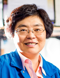
To Ruxin Li of the Shanghai Institute of Optics and Fine Mechanics, China, some of the most interesting and productive developments in laser technology have been those that have boosted average and peak laser power, which he says “significantly promote and expand applications of lasers.” A case in point: The Station of Extreme Light (SEL) that Li and his team are developing in Shanghai.
Li says that the SEL project—approved by the Chinese government in 2017, and kicked off in spring 2018—has most of its engineering design completed, and the facility front end is now being developed. The ultimate goal will be a laser capable of pulses carrying a peak power of 100 PW—around an order of magnitude greater than those of the most powerful lasers operating today—and a focused intensity of more than 1023 W/cm2. The current schedule envisions completing the facility, and opening it to users, in 2025.
Once the facility is online, the “day-one experiment,” according to Li, will be putting pulses from this powerful laser together with hard-X-ray pulses from an X-ray free-electron laser, for pump–probe experiments to investigate vacuum birefringence. That’s a phenomenon predicted by strong-field quantum electrodynamics, in which the quantum vacuum behaves like a sort of prism owing to the presence of “virtual” particles within it. Verifying this strange non-emptiness of the vacuum would mark a significant scientific milestone for SEL. Also on the table, according to Li, is using the laser to generate high-energy particles and radiation for a variety of applications.
To push things still further, Keller’s team is focusing on the repetition rate for these ultrafast lasers. One way (in addition to XFELs) to create attosecond pulses is to fire few-cycle, femtosecond laser pulses through a gas target to drive high-harmonic generation, or HHG (see OPN, May 2015). But HHG is an inefficient process, and for applications such as doing spectroscopy on attosecond timescales—experiments that can peer into electron dynamics during biochemical reactions—there’s a significant need to boost average power.
“The signal to noise in those kinds of measurements goes with the average photon flux,” Keller explains. And in many kinds of experiments, the best way to improve that average flux is to boost the rate of nanojoule-scale attosecond pulses.
In work published in February 2020 in Optica, Keller’s ETH Zurich team presented a system using optical parametric chirped-pulse amplification (OPCPA) that could push out mid-IR, few-cycle laser pulses with 14 GW peak power at a rate of 100,000 pulses per second—and used those pulses to drive HHG production of coherent attosecond soft X-rays. The 100-kHz rep rate was two orders of magnitude higher than the rates of the sources typically used in such experiments. That’s a potentially huge gain in signal to noise that could, according to the paper, enable “a new generation of attosecond studies.”
Looking back today, Keller says she “never could have predicted how fast progress would be in attosecond science, and in the average power scaling of the lasers. It’s just amazing where we are.”
Going small
The business end of Maiman’s 1960 laser could be held in the palm of one’s hands. That’s a far cry from the enormous, football-field-scale terawatt and petawatt laser complexes of the U.S. National Ignition Facility and Europe’s Extreme Light Infrastructure (see OPN, January 2020), and the 100-PW Station of Extreme Light being built in China (see “Platforms of Power,” right). But some of the laser’s biggest impacts, particularly in communications, have come from efforts in the opposite direction—to make lasers very small.
One success story has been the vertical cavity surface-emitting laser (VCSEL), originally pioneered in the late 1970s by Kenichi Iga of the Tokyo Institute of Technology, and now a fixture in everything from computer mice to short-run interconnects in data centers. Constance Chang-Hasnain of the University of California Berkeley, USA, attributes their success to two factors: a “nice, usable beam” that’s easily guided and coupled to other devices, and wafer-scale manufacturing, analogous to that of LEDs. “Once you master the fabrication of one,” she says, “you can make tons of them.”
[Noah Berger]“VCSELs are extremely scalable. Once you master the fabrication of one, you can make tons of them.”
—OSA Fellow Constance Chang-Hasnain
Chang-Hasnain became involved with VCSELs by being “in the right place at the right time,” working in the late 1980s at Bellcore, the New Jersey–based research arm of the former Bell Telephone operating companies in the United States. There, she contributed to the second generation of VCSEL development, driven by advances in the fabrication and physics of semiconductor devices.
Today, the growth of 3D-sensing modules in smartphones has set VCSELs up for another explosion of growth. The firm Yole Développement recently projected that the market for these sensors could quadruple, from US$2 billion to US$8.2 billion, between 2019 and 2025. VCSELs constitute a core enabling technology for such sensors—in part, according to Chang-Hasnain, because previous demand and mass-production requirements for other applications made the technology ready to feed this emerging new market.
Chang-Hasnain’s team, meanwhile, continues to push VCSEL technology further. One recent emphasis has been VCSELs featuring high-contrast gratings, which can replace the thick stack of distributed Bragg reflectors in VCSEL designs, cutting the device thickness by around 50%. That, she explains, also makes it easier to manufacture the lasers, and to integrate them into flexible MEMS devices. Such devices, she notes, are already making headway in opthalmology and have potential in real-time imaging to guide precision surgery. “It’s very exciting,” says Chang-Hasnain.
Another avenue for exploiting the power of small lasers lies, of course, in integrating them on silicon chips. Such laser integration, according to John Bowers of the University of California, Santa Barbara, USA, “allows a much more complex integrated circuit” that can be pressed into service in high-bandwidth data communications, lidar, and even exotic applications such as compact laser gyroscopes for rotation sensing. “Today, laser gyroscopes are $10,000 each,” says Bowers. “They go on airplanes, but they don’t get applied to your car or cellphone … If we can integrate the laser and the whole photonic circuit on the chip, and do it in high volume in silicon, it becomes competitive and allows new applications to enter.”
[UC Santa Barbara]“If we can integrate the laser and photonic circuit on the chip, in high volume in silicon, it allows new applications.”
—OSA Fellow John Bowers
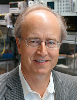
Traditionally, silicon’s indirect band gap, which makes it an extremely poor emitter, has been a stumbling block to getting lasers on the material. But Bowers, who will give a plenary talk on the subject at this month’s CLEO Conference, says enormous progress has been made. Heterogenous integration—in which a direct-bandgap, highly efficient light-emitting “III–V” material is bonded to a silicon wafer and then processed in a conventional CMOS facility—is already well established, with more than two million transceivers per year reportedly being produced by Intel alone.
Laser integration via another process, epitaxial growth, has been tougher—but looks “very promising” for the future, Bowers says. He cites recent experiments that created epitaxially grown lasers on silicon with lifetimes of 100 million hours at room temperature. The key to these lasers, he explains, is creating the laser’s active region using luminescent nanoparticles, or quantum dots, which avoid some of the materials-defect problems that have hobbled other approaches to growing lasers via epitaxy. The work is, in Bowers’ estimation, “probably lagging 10 years behind” heterogeneous integration. But it’s worth pursuing, as it could make lasers on silicon “incredibly cheap,” priming still more applications.
Even smaller: Nanolasers
Still smaller lasers have also captured scientific and industry attention—so-called nanolasers. These, explains Teri Odom of Northwestern University, USA, are lasers in which at least one of the relevant dimensions, such as cavity length or feedback mechanism, is on the nanometer scale, well below the diffraction limit of light. For example, in plasmonic nanocavities, light amplification takes place very close to the surface of the metal nanostructures. And lattices of nanoparticles can dramatically enhance the localized light field.
[Northwestern University/Matthew Gildon]“The laser has widened the space where many different disciplines can contribute to both fundamental knowledge and potential applications.”
—OSA Fellow Teri Odom

Odom says her involvement with nanolasers grew out of a more general interest in nanoscale light–matter interactions. “In the beginning, our goal wasn’t to say, Oh, let’s just make a nanolaser because it sounds cool,” she says. But as she and her team studied the characteristics of energy transfer between emitters, such as dye molecules and quantum dots, and plasmonic lattices, “it turned out that these systems exhibited really interesting characteristics,” such as a lasing threshold energy and directional emission, “that are reminiscent of macroscale lasers.”
In a September 2019 study in Nature Materials, Odom and colleagues at Northwestern, Lawrence Berkeley National Laboratory and Columbia University fashioned one such miniaturized laser. The device, hosted in a glass matrix, used a lattice of 50-nm-tall silver nanopillars to form the cavity. As the gain medium, the team coated the pillars with a 150-nm-thick film of upconversion nanoparticles (UCNPs)—inorganic nanomaterials doped with rare-earth ions that can convert lower-energy photons to higher-energy ones.
The result was a super-tiny laser that, when pumped with near-IR light, could produce continuous-wave emission in the visible. That combination, plus the fact that the platform is biocompatible, opens up opportunities in deep-tissue imaging, sensing and optogenetics. That’s because the device can be stimulated by near-IR pump light—which can be delivered externally and penetrate biological tissues—to produce, via the UCNPs, visible laser light for the deep-tissue imaging and therapeutics. And the device’s low lasing threshold also creates other possibilities, according to Odom, including use as light sources for quantum applications.
Lasers, Odom concludes, have “widened the space where many different disciplines can contribute to both new fundamental knowledge and potential applications.”
Spawning an industry
As is well known, soon after Maiman’s initial laser demonstration, someone—just who is a matter of dispute—quipped that the laser was “a solution looking for a problem.” World industry clearly got the memo. In the six decades since, the laser has spawned a global market estimated by Strategies Unlimited at more than US$16.6 billion annually. And Wilhelm Kaenders, who co-founded the laser firm Toptica Photonics AG just over 22 years ago, says that, from industry’s viewpoint, the past six decades “have pushed the technology from being just a small, first dim laser light to many extremes.”
[OSA]“In many approaches to quantum computers, lasers are an indispensable tool to prepare, initialize and interrogate quantum states.”
—OSA Fellow Wilhelm Kaenders
As Kaenders observes, the laser industry’s growth reflects improvement on a huge variety of fronts, ranging from expansion of the available spectral range and improvements in stability and linewidth to the “new laser field” opened by the advent of frequency combs. One “remarkable achievement,” he says, has been the laser’s extension to an almost complete range of wavelengths, which has allowed it to penetrate a vast array of markets in manufacturing, sensing and analysis. “Most materials can today be addressed for various forms of processing … with a suitable laser source” says Kaenders, who cites some relatively new examples—cutting/ablating with UV wavelengths; welding copper with blue/green diode lasers; bioprinting with 3-µm IR laser light.
Kaenders notes that today, some venerable and well-developed lasers—such as “the ubiquitous gas lasers that were among the technologies that started the laser field”—are still “able to defend some market niches.” But those niches, he believes, may fall to direct diodes, diode-pumped solid-state lasers or fiber lasers as customers increasingly focus on compactness, efficiency, integration and cost of ownership.
In the area of medical applications, for example, Kaenders believes for ultrafast techniques like multiphoton microscopy, only fiber lasers are compact, convenient and efficient enough to drive the transition of applications from research labs to the clinic—even solving the light-delivery problem as part of the design. One other example he cites is “multi-laser engines,” in which one unit provides different colors to drive diverse applications such as microscopy, cytometry and DNA sequencing: A unit that once required “a cubic meter of space and kilowatts of electrical power,” Kaenders says, can now “be served out of a shoebox-sized device.”
In a somewhat more exotic vein, Kaenders also sees potential in the emerging market for quantum technology. “In many approaches to quantum computers,” he says, “lasers are an indispensable tool to prepare, initialize and interrogate quantum states,” as well as for linking quantum processors together in networks. For current experiments in quantum technology involving trapped ions or atoms, he observes, today’s lasers seem equal to the task, providing the needed tunability and optical phase control. “The challenges for the future are more like how to get these lasers out out of the lab—ultra-compact and transportable, but still high performing,” says Kaenders.
Whirlwind trip
With talk of quantum computers and information networks, we have come a very long way from Theodore Maiman’s May 1960 lab benchtop. Even so, for an invention as fruitful as the laser, a whirlwind trip such as this story is inevitably an exercise in frustration, given how much must be skipped along the way. Unmentioned here have been the myriad applications opening up for lasers in outer space; the ultrastable lasers that enabled the first detection of gravitational waves; a vast array of active application areas in medicine, science, industry and the military; and countless other efforts to take lasers to the next level. We’ve put together an online library of OPN content (www.osa-opn.org/link/laser-at-60) for those seeking a deeper dive.
For now, we’ll leave the last word to Robert Byer, who—having seen and contributed to laser science since its beginning—is unusually well positioned to appreciate the changes presaged by Maiman’s May 1960 demonstration. Alluding to the notion of the first lasers as “a solution looking for a problem,” Byer notes that the laser subsequently “found a set of problems to solve that are global in extent. All of our communication today is based on laser and optical-fiber communication. Lasers have penetrated virtually all fields of science and medicine.”
“The sixty years,” says Byer, “have gone by pretty quickly.”
OPN thanks OSA Fellows John Bowers, Robert Byer, Federico Capasso, Constance Chang-Hasnain, Jeff Hecht, Wilhelm Kaenders, Ursula Keller, Ruxin Li and Teri Odom for their assistance with this feature.
Stewart Wills is OPN’s senior editor.
Visit www.osa-opn.org/link/laser-at-60 for longer Q&As with the OSA Fellows interviewed for this story; references and resources; and links to previous OPN features on laser history and science.
Editor's note:A correction was posted on this article on 12 May 2020.