
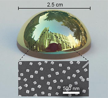
A curved surface, decorated with nanoscale silver cubes atop a gold film, acts as a near-perfect absorber of red light, which accounts for the greenish tinge of the reflected light from the surface. [Image: Maiken Mikkelsen and Gleb Akselrod, Duke University, USA]
Spectrally selective light absorbers are used in a wide range of advanced photonic applications—but producing large-area metasurfaces for near-perfect absorption has been an expensive proposition. A team of scientists from Duke University, USA, has now reportedly come up with a simple, scalable chemical technique for creating such metasurfaces, using deposition of silver nanocubes atop a layered metal-polymer foundation (Adv. Mater., doi: 10.1002/adma.201503281). The result, according to the team, is “truly macroscopic,” near-perfect-absorption metasurfaces that are tunable from the visible to the near-infrared—and that could find application in photodetectors, imaging sensors and other devices.
Beyond paints and dyes
Naturally occurring dyes and pigments show up in materials from paints to food coloring, but the absorption tends to be weak and splayed across a relatively broad range of wavelengths. Advanced photonic applications such as hyperspectral imaging generally require more complete and narrowband absorption.
One route to creating such perfect narrowband absorbers is to take advantage of plasmonic effects, using metasurfaces decorated with nanoscale metallic elements at subwavelength separations. The nanoscale elements can act as resonators, leading to complete absorption of narrowly selected wavelengths, depending on the specific geometry and arrangement of the elements. The problem is that creating such metasurfaces has tended to rely on “top-down” patterning techniques such as electron beam lithography to achieve the significantly subwavelength scales required. That makes it very costly to scale up production to the large (and sometimes curved) surface areas required in some applications.
Better metasurfaces through chemistry
The Duke team, led by OSA Member Maiken Mikkelsen, decided to look at the problem of creating perfect absorbers from the bottom up, bypassing expensive lithography in favor straightforward chemical techniques. The researchers began by depositing a 75-nm-thick gold film atop an ordinary silicon wafer, and then dip-coating the film with a polymer spacer of less than 10 nm thickness, a process that leaves the film with a positive net charge at the top. Next, they used a similar simple, immersion-based method to cover the film with a layer of tiny silver nanocubes, which had been created in solution via a well-established chemical techniques. The negatively charged cubes stick electrostatically to the positively charged polymer, creating the decorated metasurface.
In putting the metasurface through its paces using lasers at various wavelengths, the team found that it showed strong, precise absorption—on the order of 99.7 percent—at the specific resonant wavelength dictated by the nanocube geometry and polymer thickness. That wavelength, moreover, could be easily tuned by adjusting the size of the cubes and the thickness of the polymer spacer (which, in turn, changes the effective size of the resonant cavity between the silver cubes and the gold base). And the simple, solution-based approach allows the absorbers to be assembled, according to the scientists, “over surfaces of arbitrary size and shape.”
Next step: harvesting hot electrons
The combination of precise spectral selectivity and large-area fabrication could, according to the Duke researchers, make the new metasurfaces directly applicable to incorporation into imaging and photodetection technologies. They also raise the prospect of creating more active devices—such as highly sensitive infrared imaging systems—by integrating the metasurfaces with semiconductors and harvesting the “hot” electrons generated in the metal resonators to generate an electrical signal. “That’s the next step,” says postdoc and lead author Gleb Akselrod.