
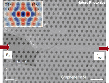
Graphene-clad silicon photonic crystal nanostructure. SEM photo shows the tuned photonic crystal cavity, partly covered by a graphene monolayer. Scale bar, 500 nm. Inset: calculated electric field.
Graphene on silicon photonic crystals could be the basis for next-generation integrated high-speed communications and all-optical signal processing. Tingyi Gu and other researchers at Columbia University (U.S.A.) and the Institute of Microelectronics in Singapore report three results from graphene-silicon hybrid optoelectronic devices operating at low energy: resonant optical bistability, self-induced regenerative oscillations, and coherent four-wave mixing (Nat. Photonics, doi: 10.1038/nphoton.2012.147).
“We have been able to demonstrate and explain the strong nonlinear response from graphene,” explains Gu. The researchers made a photonic crystal from a silicon membrane, with a line defect and a nanocavity (consisting of three missing holes) side-coupled to a line defect. Then they transferred a large monolayer graphene sheet onto the membrane surface. The heavily doped graphene, grown by chemical vapor deposition, was designed to be transparent in the infrared (IR). When polarized laser light was launched into the optical cavity, some of it was evanescently coupled into the graphene layer.
Using this device, Gu and her group showed bistable switching with low thresholds under a milliwatt. At higher input powers, the behavior changed: the output started oscillating, generating a microwave frequency on top of the laser beam. The microwave output was controllable by changing the laser intensity and wavelength.
And the processes worked at cavity recirculating energies of only a few femtojoules. The graphene-silicon hybrid chip generated the microwaves much more efficiently than other silicon devices. “Showing the power-efficiency of this graphene-silicon hybrid photonic chip is an important step forward in building all-optical processing elements that are essential to faster, more efficient, modern telecommunications,” says Gu.
Xiang Zhang, director of the National Science Foundation Nanoscale Science and Engineering Center at the University of California, Berkeley, commented, “this new study in integrating graphene with silicon photonic crystals is very exciting. Using the large nonlinear response of graphene in silicon photonics demonstrated in this work will be a promising approach for ultra-low power on-chip optical communications.”