
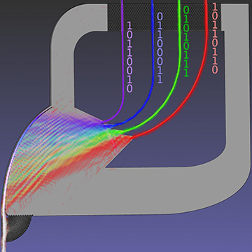
Researchers at Osaka University and the University of Adelaide have demonstrated an integrated multiplexer that funnels terahertz data streams in four frequency bands from a waveguide to different points on a silicon slab. [Image: Osaka University]
With frequencies tens or hundreds of times higher than those used by today’s wireless communication networks, terahertz waves offer the potential of exceptionally large bandwidths for data transfer. But making suitable transmitters and other components in this portion of the electromagnetic spectrum has to date proved a huge challenge.
Researchers in Japan and Australia have taken a small step toward realizing the necessary technology by demonstrating a new kind of integrated terahertz multiplexer. They have shown how to separate incoming data into four distinct frequency channels at speeds of several tens of gigabytes per second using a silicon slab several orders of magnitude smaller than those of rival devices (Optica, doi: 10.1364/OPTICA.420715).
Terahertz roadblocks
A major stumbling block in the application of terahertz radiation is its very limited range in air—radiation in this band being readily absorbed by water vapor and oxygen. This problem could potentially be alleviated by using transmitters with suitably high power output and efficiency, but device performances to date have proved disappointing.
One way to try and maximize power is by combining the output from several devices operating at different frequencies. However, direct frequency-division multiplexing of terahertz waves is tricky, with few promising schemes so far. One option is to use free-space optics to gather radiation from a leaky-wave antenna, but the necessary components are bulky. Hollow metallic waveguides can instead be used to make diplexers, but such devices are fairly complicated to build.
A silicon solution
In the latest work, Masayuki Fujita and Daniel Headland of Osaka University, Japan, and colleagues have demonstrated a new kind of scalable photonic multiplexer made from silicon. Typically, such multiplexers involve arrays of waveguides connected to a dielectric slab, but these devices are relatively large—to operate at 300 GHz, they would occupy an area of about 2000 cm2.
Fujita and colleagues instead exploit the phenomenon of optical tunneling to tap radiation from an unclad silicon waveguide. Usually such a waveguide would confine energy within its transverse electric mode and thereby remain insulated from the environment. But when placed close to a dielectric slab, its evanescent fields couple to the slab, causing it to progressively leak terahertz radiation.
The idea is to shape the interface between waveguide and slab such that radiation from all points along the edge meet at the same point within the slab. Since the location of that point varies with frequency, broadband terahertz radiation from the waveguide will fan out across the slab according to frequency. By funneling the waves towards a few specific points on the far side of the slab, the radiation can be split into a number of distinct bands.
Promising data rates
Using computer simulations and deep reactive-ion etching, the researchers designed and built a multiplexer with a curved interface from a piece of silicon with a footprint of just 4 cm2. The waveguide and slab are separated by a tiny air gap that gets smaller and smaller along the curve (to compensate for progressive leaking of radiation), while the funneling is done by carving out four “flares”—each connected to a separate output waveguide.
Fujita and coworkers put their device to the test by exposing it to terahertz waves between 300 GHz and 390 GHz, and then measuring its down-converted output with a spectrum analyzer. They found it successfully split the radiation into four distinct bands with an efficiency and bandwidth “comparable to simulation” (although they say that over-etching shifted the output of each channel upwards by about 10 GHz).
They then investigated whether the multiplexer is suited to its intended application—communication. They did so by using a digital pulse generator to modulate the output of an infrared laser via simple on/off switching, and then transferring that modulation to the terahertz range by recording the laser’s beat frequency. They found that all four channels supported data rates of several gigabits per second, and that a maximum error rate of 1 in 1000 yields an overall capacity of 48 Gbits/s (although they say that this could be improved upon using more sophisticated modulation schemes).
Countering crosstalk
However, this experiment involved testing one channel at a time. The researchers point out that running the channels simultaneously would introduce the problem of crosstalk, and calculate theoretically a signal-to-interference ratio of 10–20 dB. Being “likely to adversely impact the quality of communications links,” they say that this problem must be countered by better isolating the multiplexer—which, they suggest, could be done by using special filters or changing the spacing between channels.
What’s more, the experiment was limited by the fact that the multiplexer was connected to both source and detector by waveguides—not via free space. Fujita and colleagues say that this shortcoming could be removed in future demonstrations by connecting advanced antennas to the device, noting that “achievable data rates will be affected in such a wireless communications link, owing to the atmospheric absorption of terahertz waves.”
Fujita adds that being able to integrate active devices including sources, detectors and modulators, as well as the packaging technology, will be a “very important” next step in the development of compact practical terahertz systems.