
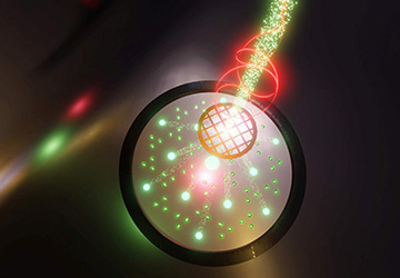
At the heart of the imaging technique is a complex array of 72 circular apertures. [Image: Murat Sivis]
In a movie-first, researchers in Germany say they have imaged light-induced phase changes in a material as they happen at atomic scale (Science, doi: 10.1126/science.abd2774).
The research team—led by Claus Ropers, University of Göttingen and the Max Planck Institute for Biophysical Chemistry, Germany—used ultrafast transmission electron microscopy (UTEM) with a tailored aperture, to capture femtosecond images of the material’s charge density wave (CDW) phases transforming with the application of light.
Understanding light-induced changes
The ability to see and control such light-induced changes in materials and devices, the researchers say, may be a game-changer for advancing current and future technologies. They cite, for example, data-storage devices, neuromorphic computing, photonic circuits, energy conversion and more.
To develop optical-control schemes for materials on the nanoscale, says first author and Göttingen doctoral student Thomas Danz, one needs to understand how light-induced changes evolve in space and time. “Our study offers a first glimpse of what complex dynamics we will be able to visualize in the future,” says Danz.
Moreover, says Ropers, “We are continuously trying to push the limits of recording ultrafast movies on the atomic scale.” The motivation for this work, he explains “is both to advance measurement technology and to learn about the fundamental behavior of materials when excited out of equilibrium.”
Harnessing control of time and space
But to harness optical control of materials, scientists need access to both nanometer-length and femtosecond time scales to see and understand what is happening.
UTEM—a method for atomic-scale imaging implemented at the University of Göttingen—presented a solution. It employs an electron beam, generated by a laser, to take snapshots of a sample. The method has proven useful, for example, in studies of lattice dynamics, which probe the vibrations of atoms in crystals. But this capability alone would not reveal subtle changes in the CDW of a sample, the team says.
Dark-field imaging with a tailored aperture
For making movies of light-induced phase changes, Danz says, “It is important to precisely understand and tailor the image contrast using beam-shaping approaches.” In conventional dark-field (DF) imaging, he explains, this is done by introducing a single circular aperture into the diffraction plane of the microscope.
But the brightness of pulsed electron beams is inherently limited, explains Ropers, and so the researchers needed a new approach. Instead of a single DF aperture, they used a tailored array with 72 individual apertures. This mask filters out all scattered electrons from the sample to transmit just the diffraction peaks of the material’s CDW phases, Ropers says. Forming a real-space image from the electrons, they were able to record the changing structure under the influence of light—the phase transition.
“We observe the formation, stabilization and relaxation of CDW domains after optical excitation and identify drastic differences between the emerging domain patterns for continuous-wave and pulsed illumination,” the team writes.
New approach to UTEM
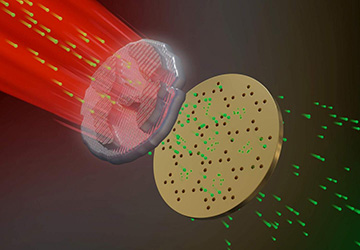
Artist's impression of the charge density wave in the ultrafast transmission electron microscope. [Image: Florian Sterl (Sterltech Optics)]
“Our UTEM instrument is the first to use a nanometric tip emitter, which is great for the quality and focus-ability of the pulsed electron beam,” says Ropers. The resulting exceptional beam quality “enables us to use the tailored DF aperture array without losing too many electrons that carry the desired image information,” he adds.
In the future, Ropers says, the team envisions the UTEM instrument being used not only to combine classical TEM imaging with femtosecond or even attosecond time resolution, but also to connect to new fields of research, such as quantum optics with electron beams.
The best material for the show
For their movie, the researchers used a type of transition metal dichalcogenide called tantalum disulfide. This transition metal, Ropers explains, has outstanding properties, including a rich variety of CDW phases, in which the crystal is slightly distorted in a wavelike fashion.
The wavy structure changes as a function of temperature and applied light intensity, Ropers says. These structural changes go along with a drastic variation in electrical properties like resistivity, representing a metal-to-insulator transition, making them interesting for future nano-electronic applications. Some of the tantalum disulfide phase transitions happen close to room temperature, which according to Ropers made it an ideal choice for the team’s proof-of-principle experiment.
Other phase-changing materials that might be imaged, Danz says, are closer to actual technological applications—for example, vanadium dioxide in intelligent window coatings, or germanium-antimony-tellurium for self-learning neural networks.
Promising sequels
The team’s approach will have greatest utility wherever insights into subtle structural changes determining the behavior of nanoscale devices are required, says Ropers. “The crystalline structure is the backbone of a material, upon which the electrical and magnetic properties and functions play out,” he explains. “To control those functions, a thorough understanding of the behavior of the crystal lattice is important.”
An exciting next step in the team’s research, Ropers says, would be simultaneous imaging of multiple coexisting phases in the same material. Furthermore, the team envisages changing the sample environment: “Imaging of optically triggered currents would be going one step further toward the ultrafast real-space imaging of nano-electronic devices,” he says.
Another possibility might be to confine the optical excitation more strongly to small volumes and move it across a sample. “In this way,” says Ropers, “one could probe more freely the resulting changes to the material, depending on where it was excited.”