
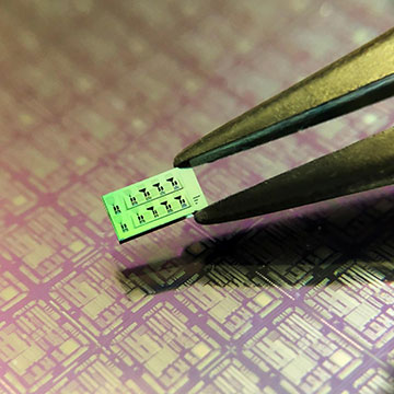
Researchers in Germany have made four silicon-on-insulator chips measuring just a few millimeters squared, each containing eight tiny ultrasound detectors that are too small to be seen with the naked eye (although their photonic interconnectors are visible). [Image: Helmholtz Zentrum Muenchen / Roman Shnaiderman]
Ultrasound provides images of otherwise hard to view objects, such as organs inside the human body, without the complications of ionizing radiation. But invaluable as it is for medical purposes, ultrasound imaging has its resolution limited by the minimum practical size of the piezoelectric transducers used to pick up the reflected sound waves.
Now, researchers in Germany have shown how to overcome this limit by exploiting the effect of ultrasound on light waves confined inside an extremely small resonator (Nature, doi: 10.1038/s41586-020-2685-y). Their new approach, which relies on the well-established silicon-on-insulator technology, is able to resolve features far smaller than the acoustic wavelength employed in the imaging.
Enhancing resolution
Measuring distance and creating images using ultrasound involves deflecting high-frequency sound waves off boundaries between materials such as different biological tissues and then recording how long it takes those waves to arrive back at a detector. Usually the detector elements rely on the piezoelectric effect, which generates electric charge in certain materials that are subject to mechanical stress. However, the sensitivity of these devices diminishes quadratically as their area decreases.
Scientists have investigated numerous optical schemes for enhancing this resolution. One approach involves using a laser beam to measure the changes in a material's refractive index brought about by variations in applied mechanical pressure. Alternatively, sound waves can be registered thanks to the changes they induce in optical interference patterns. But here too, resolution has its limits—microring resonators and Fabry-Pérot etalons, for example, being unable to confine light to a space smaller than around 50 μm.
The SWED solution
In the latest work, Vasilis Ntziachristos and colleagues at the Technical University of Munich have reached sub-micron resolution in devices fabricated using two layers of silicon dioxide separated by a 220-nm-thick layer of silicon. Each device consists of a single waveguide containing a 320-nm-long optical cavity bounded at both ends by mirrors—one a very short Bragg grating of variable length capped by a reflective silver layer, and the other a longer, fixed grating. The waveguide's cross-section measures just 220 nm by 500 nm, making it the world’s smallest ultrasound detector, according to the team.
Continuous-wave laser light that is tuned slightly off the cavity’s resonance is pumped into the cavity, where it is reflected back toward a photodiode and recorded by an oscilloscope. Sound waves passing through the cavity create pressure fluctuations that very slightly expand and contract the cavity, which in turn shift the resonance and change the amount of light reflected from the cavity.
Ntziachristos and colleagues used high-throughput techniques from the semiconductor industry to fabricate four silicon-on-insulator chips, each about 10 mm2. On every chip, they used ultraviolet lithography to fabricate eight devices, which they refer to as silicon waveguide–etalon detectors (SWEDs), at intervals of one every 10 microns.
The German group put its SWEDs to the test by exposing them to ultrasound waves generated by focusing pulsed laser beams onto thin films of gold and vinyl. The device demonstrated not only a very large detection bandwidth—up to 230 MHz—but also sub-wavelength resolution. It recorded images of a tiny metallic mesh, showing the width of the constituent filaments to be about 9 μm—agreeing with images of the same object taken by a high-end optical confocal microscope. On the basis of these images, the team estimated the SWEDs' resolution to be about 650 nm—some 50 times smaller than the acoustic wavelength in question, which was about 33 μm.
Toward biomedical applications
The researchers say that their new detector design has a sensitivity per unit area 1000 times greater than that of microring resonators and a whopping 100 million times that of piezoelectric devices. Using currently available manufacturing processes to lower the distance between SWEDs on a chip and reduce the thickness of their silicon wafer, they reckon they should be able to cram in more than 1000 detectors per square millimeter—orders of magnitude more than rival technologies.
They point out, however, that they have challenges ahead. For one thing, they say, it will be hard to supply light for large numbers of resonators using a single laser given differences in the cavity dimensions brought about by variations during the manufacturing process. But the researchers believe they might be able to solve this problem by placing on-chip photodetectors and tunable Mach-Zender interferometers alongside the SWEDs.
The researchers envisage their new technology potentially being used for a wide range of medical and industrial applications, as well as perhaps enabling new insights into the fundamental properties of ultrasonic waves themselves. To get started, they are recording images of biological cells and narrow blood vessels using laser-generated acoustic waves—a major focus of their research.