
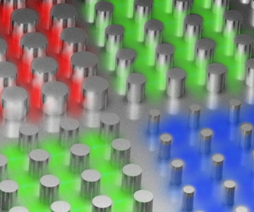
Detail view of a nanopillar-dotted metasurface mirror. The meta-mirror lies at the heart of what U.S. and Korean researchers say is a “fundamentally new device architecture and fabrication approach” for creating OLED displays. [Image: Samsung Advanced Institute of Technology]
Organic light-emitting diodes (OLEDs) have carved out a lucrative market in digital displays ranging from smartphones to large-screen televisions. But the close-to-the-eye screens of emerging applications in augmented reality and virtual reality (AR/VR) need to pack in thousands of pixels per inch (ppi), and manufacturers of OLED-based displays have thus far been unable to meet that density requirement. That’s a pity, since other characteristics of OLEDs—particularly their light weight, flexibility and brightness—would make them a great fit for AR/VR applications.
Now, researchers from Stanford University, USA, and Samsung Electronics and Hanyang University, Republic of Korea, appear to have broken through the pixel-density barrier in spectacular fashion, devising an approach that can take OLED displays to 10,000 ppi and beyond (Science, doi: 10.1126/science.abc8530). The secret ingredient: a clever use of an engineered metasurface mirror that boosts the brightness of OLED pixels—while allowing their practically manufacturable sizes to be scaled way down.
Current shortcomings
In large-scale manufacturing, OLEDs are generally made in one of two ways. For small-form-factor, high-res screens like those on modern smartphones, the organic film is laid on fine-metal masks (FMMs) dotted with thousands of tiny holes, to create red, green and blue sub-pixels that together form an individual pixel. For larger-form-factor displays like TVs, this method isn’t practical, as the FMM tends to sag across large areas. So these larger units instead commonly are constructed using white OLEDs, with color filters over the diodes employed to determine the final sub-pixel color.
Both approaches, however, have built-in limits to resolution, along with other disadvantages. Pixels produced with FMMs can go only so small before a “shadowing” effect sets in that degrades image quality. And filter-based white-OLED displays suffer optical losses of 70%, which makes them power-hungry. They can also fall prey to the dreaded phenomenon of “burn-in,” in which a ghostly relic of a displayed image like a persistent news ticker or scoreboard can become a permanent feature of the display.
AR/VR seeks a higher density
These disadvantages have held down OLED display resolutions to around 400–500 ppi for smartphones, and 100–200 ppi for large-screen TVs. Those numbers are an order of magnitude too low for AR/VR micro-display applications. That’s because these AR/VR screens sit very close to the eye, which boosts the pixel-density requirements into the thousands for a crisp, full-color view.
The team behind the new research, led by OSA Fellow Mark Brongersma at Stanford and Won-Jae Joo at Samsung, sought a way around this conundrum. The solution they came up with combines a venerable optical concept—the resonant Fabry-Pérot cavity, to boost the emission quality and efficiency of the display—with cutting-edge metasurfaces, which manage the color creation.
Nanopillar-studded mirror
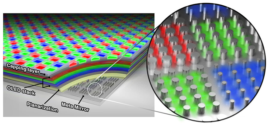
Illustration of the meta-OLED display architecture and the underlying metaphotonic layer. [Image: Samsung Advanced Institute of Technology] [Enlarge image]
The team’s OLED stack begins with a reflective metasurface mirror consisting of tiny pillars, on the order of 80 to 120 nm in size. The researchers fabricated the pillars using nanoimprint lithography on silicon, created a polymer cast of the required nanopillar structure, and then draped a 200-nm-thick silver layer on the cast to create the meta-mirror.
On top of that reflective metasurface, the researchers then deposited an indium-tin-oxide layer to serve as the OLED anode, successive blue, green and red electroluminescent (EL) layers, and an overtopping reflective silver layer to serve as the cathode. A glass capping layer rounded out the OLED structure.
The fabrication chain left the team with, essentially, a white-light OLED (owing to the additive-color effect of the stacked EL layers), sandwiched within a two-mirror Fabry-Pérot cavity—the meta-mirror at the bottom, and the partly reflective silver cathode mirror at the top. White light emitted from the EL layers bounces between the meta-mirror and the cathode. At the meta-mirror, subwavelength resonances between the components of the white light and the nanopillars on the meta-mirror amplify specific colors—red, green or blue—depending on the size and spacing of the nanopillars. When the colored light has reached a threshold brightness, it escapes through the silver cathode.
Bright, pure and dense
The team believes that the meta-mirror-based framework escapes the shortcomings of previous OLED display techniques—allowing potentially far higher pixel densities than the FMM-fabricated displays of smartphones, while escaping the optical losses and heavy power appetite of TV displays that rely on filters to create their colors.
To test things out, the researchers created a prototype display device using the meta-mirror approach. Each pixel in the display consists of four square sub-pixels; each of those, in turn, comprises a field of nanopillars tuned to amplify a specific color. The team found that the design delivered luminescence efficiencies twice as high as the white-light, color-filtered OLED displays used on TVs, with sharper spectral peaks implying better color purity as well.
The total area of the each pixel in the prototype display, meanwhile, came in at only around 2.4 µm. That’s less than one ten-thousandth of an inch, pointing to the prospect of the technology’s use to fashion 10,000-ppi, AR/VR-ready micro-displays.
A win for metaphotonics
In a press release accompanying the research, Brongersma observed that the work illustrates how nanophotonics, heretofore largely the domain of impressive accomplishments in the lab, is “starting to impact real technologies.” Indeed, the authors write in the paper that they “expect metaphotonic OLEDs to emerge as the leading technology for the next generation of microdisplays and to become one of the most practical applications of metaphotonic technology.” Engineers at Samsung are now working to integrate the technology into a full-sized display.