
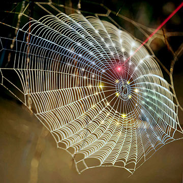
A spider-web-inspired fractal design is used for hemispherical 3D photodetection to replicate the vision system of arthropods. [Image: Sena Huh/Purdue University]
Like poets and painters, scientists are often inspired by nature. In a recent example, researchers have taken inspiration both from the webs and compound eyes of spiders to create a 3D photodetection system with a large field of view and no aberration (Adv. Mater., doi: 10.1002/adma.202004456).
Natural engineering solutions
Compound-eye-mimicking designs are very attractive for 3D optoelectronics, particularly for photodetection systems that require a large field of view and wide-angle reflection. But assembling high-performance optoelectronics onto curved microlenses has become an engineering stumbling block, impeding progress toward 3D photodetection systems that could benefit biomedical and military imaging applications.
To tackle this challenge, the team—comprising researchers from the United States, India and South Korea—considered the fractal design of spider webs, which has long fascinated engineers thanks to the repeating pattern’s unique ability to distribute stress and tolerate damage while maintaining strength and function.
“Nature-inspired engineering designs often play an important role to solve challenging problems,” explains co-author Chi Hwan Lee at Purdue University, USA. “The novelty of our work arises from the fact that we have learned from the fractal design of spider webs to develop a 3D photodetection system that mimics the vision system of arthropods, allowing for a larger field of view with no aberration.”
Doping graphene
To construct their photodetector, Lee and colleagues developed an organic-dye-sensitized graphene hybrid composite. Graphene—the celebrated, atomically thin 2D version of carbon—offers superior optoelectronic properties and mechanical flexibility compared with alternatives like silicon. Graphene’s photosensitivity, however, is limited by its atomic thinness. The hybrid composite material developed by the researchers enhanced the material’s optical absorption, overcoming this limitation.
The team began by microfabricating the photodetector array on a standard 2D silicon wafer. Using a wet transfer printing technique, the array was then assembled on a transparent hemispherical dome. The final design comprised 48-pixel photodetectors at the cross-junctions of the spiral and radial threads of the webbed array. The team writes that increasing the amount of spiral threads, radial threads or both while maintaining the device size would further improve the array’s spatial resolution.
In experiments, Lee says, the 3D photodetector demonstrated not only advanced optoelectronic functionality in detecting both direction and intensity of light, “but also superior photoresponsivity, compared to other similar counterparts, through the use of a graphene hybrid composite as a flexible and effective photoactive component.”
The fractal design provided mechanical resilience as the researchers repeatedly attached and detached the device from planar and curved surfaces. Throughout these characterizations, the researchers write, the device’s photocurrent remained nearly unchanged at 653–666 μA.
Optoelectronic applications
“Our work establishes a platform technology that can integrate a fractal web design with system-level hemispherical electronics and sensors,” says Lee, “thereby offering excellent mechanical adaptability and damage-tolerance against various mechanical loads (like spider webs do).” Moreover, Lee suggests, the team’s assembly technique could foreshadow new opportunities for advancing 3D electronic and optoelectronic devices.
The team has filed a patent for its technology and is seeking partners moving forward.