
John Bowers. [Image: UC Santa Barbara]
For its May 2020 print article “The Laser at 60,” OPN interviewed a range of OSA Fellows to get their insights on some particularly interesting horizons in laser research today. We’re presenting a selection of those interviews online. Below is an edited version of our interview with John Bowers, a professor and the director for the Institute for Energy Efficiency at the University of California, Santa Barbara, USA. Bowers will give a plenary talk on the prospects for silicon photonics at the virtual CLEO 2020 conference on Tuesday, 12 May.
This might seem kind of an obvious question to start with, but: why is it important to get lasers integrated on these chips—what sort of things is that accomplishing, and what sort of applications is it driving?
I think it enables a much more complex integrated circuit. If you just have a single laser driving something, then integration is not required. Integration allows a much richer, more complex set of photonic integrated circuits and addresses a much broader set of applications.
As an example, a while back, we did a 2.56-terabit chip that had 64 channels. If we didn’t have the 64 lasers integrated on that chip, that would have been impossible, right? And I think we’re seeing more and more examples of that—whether it’s in datacom or telecom or LIDAR.
Optical gyroscopes are another example—for rotation sensing for automobiles and planes and everything else. Lasers give you a better sensitivity that you get with MEMS devices, but you have to get to the MEMS sort of pricing to be competitive. So integration of the laser with the rest of that device for a gyroscope is essential.
Today, laser gyroscopes are $10,000 each. So they go on airplanes, but they don’t get applied to your car or your cellphone and things like that. But if we can integrate the laser and the whole photonic circuit on the chip, and do it in high volume in silicon photonics, it becomes competitive and allows new applications to become interesting.
My understanding is that in silicon photonics, the laser integration has been one of the more difficult aspects of it, because silicon itself is such a poor emitter. Could you talk about some of the challenges?
The basic problem, as you said, is that silicon has an indirect band gap, so its emission efficiency is literally only about one photon per million electrons that you inject. However, for all these applications, particularly interconnects, you need low power, so you really need efficiencies, that are certainly better than 10% and ideally 50% or higher.
To compete against VCSELs for interconnects, you really have to get pretty efficient emitters to do so. And we are, in fact, now seeing a large fraction of the transceivers going into data centers are now based in silicon photonics. Because when you integrate the laser, you can now combine multiple wavelengths, do WDM and get to ever-higher data rates. That’s difficult to achieve with a VCSEL, because it’s difficult to make WDM arrays and also difficult to integrate that into a single waveguide. With in-plane technology with laser integration on it—conventional silicon photonics—it becomes fairly simple to do.
So how does the integration of the laser on silicon work?
The key aspect to get very efficient, very high performance lasers is to use a direct bandgap material. There are two ways to do so. One is to heterogeneously combine III-V and Si, and the other is to epitaxially grow III-V on Si.
Heterogeneous integration—where you bond the III–V material onto a silicon wafer and then process it in a conventional CMOS facility—works very, very well. Intel and Juniper and HPE are all heavily pursuing this. In a recent article, Intel mentions that they’re now at a run rate of two million transceivers per year. That’s a significant fraction of the overall market. It has high powers, operates at high temperatures, above 140 °C, and has great reliability because there are no exposed facets, which conventional semiconductor lasers have.
The other approach, epitaxial growth, has lagged, because there are reliability issues with that. When you epitaxially grow, the materials have different lattice constants, and you incorporate defects into the material. But fortunately, we’ve found that if you use active regions consisting of quantum dots, you get a very strong robustness against degradation. So at room temperature, we can now get lasers with a 100-million-hour lifetime with quantum dots epitaxially grown on silicon. And that’s very promising.
The heterogeneous approach is already in production on 300-millimeter wafers. Epitaxial growth is not there yet; it’s lagging 10 years behind. But it looks really promising for the future. The field moving very fast, and there’s lots of people working on it around the world—not just the United States, but also in Hong Kong, China, Japan, United Kingdom, and Germany .
I’m curious—if heterogeneous integration is working so well, what makes epitaxial advantageous, and worth working on?
If you do it with heterogeneous bonding, the integration is indeed fairly straightforward and very achievable, and Intel and others have done that. And you can basically do that in the back end of the process, where you’ve got copper and other things contaminating the circuits anyway. So the III–V materials are not a particularly big issue.
When you do epitaxial growth, it may need to be integrated earlier in the process. So integration with CMOS is more of a challenge; even if everything technically worked out fine, there’s more issues with integration, and we’re still working on that.
But the driver for it—the reason that it’s interesting—is that you can buy a 300-millimeter silicon wafer for a couple hundred dollars. Whereas a six-inch, 150-millimeter indium phosphide wafer of the sort you’d use for heterogeneous integration is $7,000. So there’s a big economic driver for epitaxial growth, to make lasers incredibly cheap.
There’s also, I believe, a lot of work—academic work, at least—going on in on-chip frequency combs. Is that anywhere near something that would be commercially relevant?
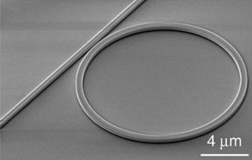
SEM image of AlGaAs-on-insulator microresonator, for on-chip freqency comb generation. [Image: L. Chang et al., Nat. Commun, doi:10.1038/s41467-020-15005-5; CC-BY 4.0]
Well, again, there’s two approaches, and each, I think, has its niche. One is to have a resonator and you pump it and it generates a comb. And so you can use silicon resonators; you can use silicon nitride, silicon dioxide, and they all work. And I think they’re close to commercialization. I think we will see comb sources—you know, know multi-wavelength sources, for things like WDM or CWDM in particular—using that approach, and I think that will be introduced in less than five years.
The competing approach is just using a mode-locked laser, which also generates a comb. So, the question is, which is lower power and more efficient? Which generates more power per line for a given pump power?
At lower free spectral ranges, mode locking is clearly better. For higher free special ranges, pumping the comb source will be a solution. We have a paper just accepted at Nature Communications on using gallium arsenide on silicon for comb generation. We get down to extremely low powers for combs—down to 30 microwatts of power to generate the comb. It used to be that you needed watts, right? And that was painful. You could do a science experiment, but you could make something practical. But now you get to something very efficient.
And again, the fact that you are doing this heterogeneously is a huge advantage. In fact, that’s the whole reason why you get the powers down from tens of milliwatts to tens of microwatts. It’s because when you take a silicon-oxide-silicon wafer and you bond gallium arsenide to it and remove the GaAs substrate, you get very high confinement vertically—and, with good lithography as you get in CMOS, good lateral confinement as well. So the area gets, really, 1000 times smaller than have in a normal gallium arsenide waveguide. And that drives the threshold powers down to just microwatt scales.
Are there any big challenges for further integration of lasers and silicon photonics, or any next frontiers that you’re seeing now?
There’s one other big change that we should note that’s happening now. Several companies—Luxtera being a prime example, and Cisco, which is now acquiring Luxtera—produce large volumes, millions of transceivers, but they use bulk optical isolators between the laser and the photonic chip. One reason is that lasers are reflection sensitive, and so you need this isolator there to perform adequately in many applications. But that kind of limits what you can do—if every laser has to have a separate bulk isolator, that’s expensive and bulky and cumbersome.
But one advantage of going to quantum dots again is that the lasers are reflection insensitive. With quantum dots you can get the linewidth-enhancement factor to be zero. And the reflection sensitivity gets better by one over linewidth enhancement to the fourth power. So even if you just get it down to 0.1, you’re 40 dB better in insensitivity.
So now I think we’ll see a whole lot of new applications come out, because this is just now being recognized. If you don’t have to have an isolator, that opens up a lot of other applications. I think this will have a big impact, and soon. It will allow us to move into other applications, like lidars and gyroscopes and things that otherwise would have required what they have today, which are isolated sources. Another new directions coming forward is using lasers and combs for things like timekeeping and precision navigation. Heterogeneous integration of visible lasers, particularly blue and UV GaN lasers, with silicon nitride waveguides on silicon was a wide range of appliations.
So I think there are many applications that will open up there, in high volume, once you can do it with low cost.
Finally, you are the director of the Institute for Energy Efficiency at UCSB. I was wondering if you had anything to say about the importance of this work—both photonic integration in general and laser integration in particular—on energy efficiency.
We’re all delighted by the growth of data centers, to solve a host of problems and to keep us from having to store all of our photos and other data on our local home computers. And increasingly, with machine learning and artificial intelligence, data centers are growing exponentially.
But if you look at electricity consumption in the United States today, data centers, the internet, etc., account for maybe 4%. At the current growth rates, particularly driven by machine learning, you’re talking about the share used at data centers growing to 25% of total electricity.
So we need to make data centers far more efficient than they are today. And that’s where photonics comes in. The energy metric that people use today is energy per bit to transmit a bit. Today that might be 10 to 100 picojoules per bit. But by integrating the laser on chip, and making more complex, higher-capacity chips, you can get that down to levels of, say, 0.1 picojoules per bit—ten or a hundred or a thousand times better than we have today.
Further, typically, in a high-performance chip today, about half the energy goes to drive the I/O. And that’s just wasteful. Whereas when you go to photonics, when you generate bits and transmit it, it doesn’t matter whether the bit goes a micron or a kilometer—it’s the same.
So it opens up other architectures for data centers. You can disaggregate memory and other things, and locate them where it makes sense, and not be limited by how far can you go before you have to regenerate the signal electrically. That’s why a big focus for us is making data centers more energy efficient than they are today.