
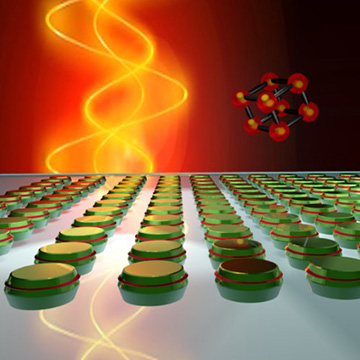
Researchers at the University of Exeter, U.K., and ITMO University, Russia, have developed dielectric metasurfaces comprising arrays of silicon nanocylinders with subwavelength-sized phase-change-material inclusions, to provide dynamic light control. [Image: University of Exeter]
The emerging, interdisciplinary science of metasurfaces has fascinated optical and photonic scientists and engineers, who see these high-tech materials as a route toward a new generation of ultracompact flat optics. But most metasurfaces demonstrated thus far have been predesigned for a single functionality; only recently have researchers begun to explore the possibilities for “active” metasurfaces that can be reconfigured on the fly.
A research team at the University of Exeter, U.K., and ITMO University, Russia, recently demonstrated one such active metasurface: a hybrid of silicon and so-called phase-change materials whose transparency and optical properties can be changed with a quick pulse of laser light (Optica, doi: 10.1364/OPTICA.384138). The researchers believe that the material could create new opportunities in lidar, ultrathin photographic lenses and other application areas.
The active-metasurface advantage
Metasurfaces are engineered materials decorated with arrays of nanoscale, subwavelength structures, on ultrathin substrates, that act as resonators or light scatterers. Properly designed, these arrays can locally change a propagating light field’s amplitude, phase and polarization. As such, the technology of metasurfaces promises to replace bulky optical components with hyper-compact elements, enabling a next generation of small-form-factor optics such as flat lenses.
In most cases, metasurfaces are designed and created as passive objects, with the changes the surface imparts to the light field frozen-in when the surface is fabricated. It’s becoming increasingly clear, however, that the development of active metasurfaces—in which the optical effect of the metasurface can be dynamically controlled—holds one key to realizing their full potential in real-world devices in wearable technology, augmented and virtual reality, imaging and a host of other areas.
Researchers are actively investigating how to tweak any of a number of variables to create such active metasurfaces. Such schemes have included systems that use electrical gating to modify the optical response of the “meta-atoms” that constitute the metasurface; the use of MEMS technology to mechanically alter the positioning and orientation of metasurface resonators, and thereby change their optical effect; chemical modification to change properties in real time; and other approaches.
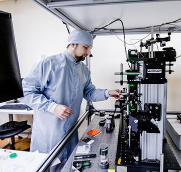
ITMO senior researcher Ivan Sinev, a coauthor on the study, in the lab. [Image: ITMO.News (https://news.itmo.ru)]
From DVDs to optically switchable metasurfaces
The Exeter–ITMO team, led by David Wright at the University of Exeter, focused on another possible approach to creating a tunable metasurface: the judicious use of phase-change materials (PCMs). As the name implies, these are materials that undergo a significant change in optical properties, such as refractive index, when the application of heat, an electric current or a laser pulse causes them to change from a crystalline to an amorphous phase (or back).
That means that PCMs might conceivably be deployed in a metasurface to allow reversible changes to the surface’s optical properties, based on a thermal, electrical or optical nudge from outside the surface itself. Indeed, a familiar storage medium, the DVD, is premised on one such PCM, germanium-antimony-tellurium (Ge2Sb2Te5, or GST for short).
GST particularly intrigued the Exeter–ITMO team because, in its amorphous state and in the 1300-to-1600-nm wavelength band, the refractive index of the material closely matches that of silicon. But in its crystalline state, GST’s refractive index sharply diverges from that of silicon. That pointed to the material’s possible use as a control switch in a silicon-based metasurface.
Real-time switching of resonance and color
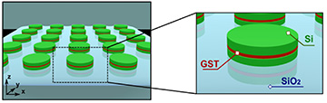
The team’s metasurface consisted of an array of silicon nanodisks, with a thin layer of a phase-change material, GST, sandwiched in each layer. [Image: C. Ruiz de Galarreta et al., Optica, doi: 10.1364/OPTICA.384138]
To build their active metasurface, the researchers used sputter deposition to lay down thin layers of silicon, GST, and silicon atop a SiO2 substrate. They then employed e-beam lithography and reactive-ion etching to carve an array of nanodisks out of the deposited layers. The result was a surface consisting of repeated ranks of 668-nm-radius, 195-nm-high disks, spaced 850 nm apart center-to-center—each of the disks consisting of pure silicon, with a thin layer of GST sandwiched in the middle.
The researchers then tested their ability to switch the optical properties of the metasurface. They found, as their modeling had predicted, that when the GST layer in the sandwich was in its original, amorphous state, the surface showed two clear spectral resonance peaks in the C and O telecom bands, as would be expected with a surface of all-silicon nanodisks. When the surface was treated to pulses from a 1050-nm, 150-fs laser, however, the GST layer was converted into its crystalline phase. That phase change, in turn, had the effect of switching off the C-band resonance—in effect, converting the surface, in real time, from a dual-band to a single-band filter.
In another set of experiments, the team numerically modeled a metasurface assuming a different dielectric material (the mineral rutile, or TiO2) and a different PCM (antimony sulfide, or Sb2S3). The result, when the position and thickness of the Sb2S3 sandwich layers was optimized, was a modeled surface that would reflect a vivid green when the PCM was in an amorphous state—but a pale, near-white light when the material was recrystallized. The calculations, according to the team, suggest the scheme’s potential for another application, the generation of reconfigurable structural colors.
The team believes that its hybrid dielectric/PCM surfaces could “provide a practicable platform for … a new generation of active optical metasurfaces with new and improved functionalities”—in applications ranging from telecom to consumer gadgets to defense.