
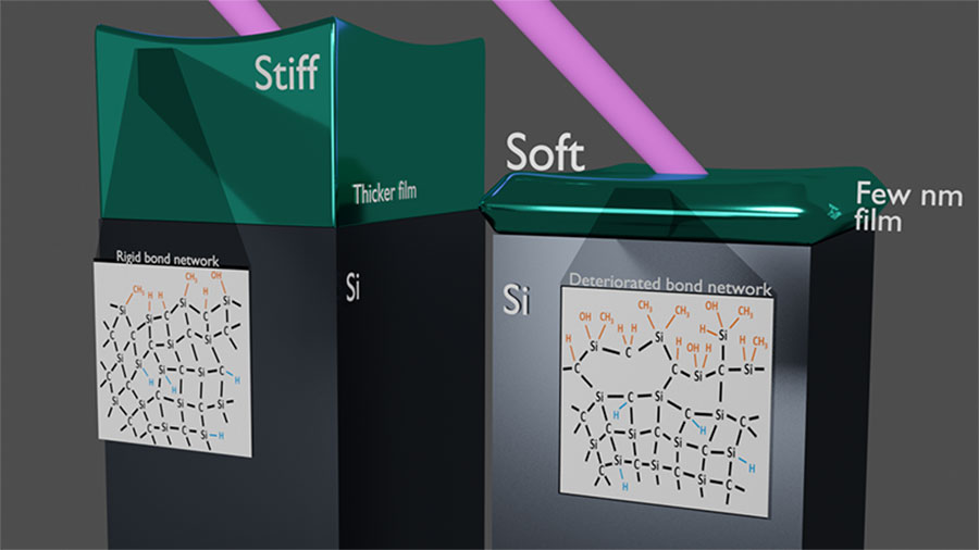
Researchers have shown that a 5-nm-thick silicon-carbide film is far softer than one roughly 50-nm-thick, owing to disruption of the material’s atomic bonds. [Image: Joshua Knobloch/JILA] [Enlarge image]
Extremely thin films of dielectrics and other materials play vital roles in many types of advanced microelectronics, but their tiny dimensions and atomic make-up can impair mechanical performance.
Now, researchers researchers at the NSF STROBE Science and Technology Center in the U.S. have shown they can characterize the mechanical properties of silicon-carbide films as thin as 5 nm using tabletop sources of extreme ultraviolet laser light—showing them to be far softer than thicker films of the same material (Phys. Rev. Mater., doi: 10.1103/PhysRevMaterials.4.073603).
Nanoscale mechanics
The mechanical properties of nanoscale-thick films can be very different than those of bulk materials owing to the relatively large number of atoms on their surface. Those atoms have significantly fewer bonds with neighboring particles in the film compared to the atoms that sit in the material's bulk, which often makes them less constrained and thereby softens the film.
However, a film's stiffness can also be altered by introducing hydrogen—which breaks bonds within the material and weakens the connectivity between atoms. This is the case for dielectrics such as silicon-carbide (SiC) or oxycarbide glass (SiOC), which can be doped with hydrogen to produce greater numbers of non-polar bonds and therefore create a lower dielectric constant—thus improving a device’s switching speed and efficiency.
Laser revelations
Travis Frazer at the JILA research center in Boulder, Colorado, USA, and colleagues have shown that they can quantify changes in stiffness by exposing these dielectrics to pairs of extremely short and precisely timed laser pulses. They did so after depositing arrays of nanoscale nickel transducers onto samples of SiC- and SiOC-covered silicon substrates made by chip manufacturer Intel. Those arrays functioned as tiny diffraction gratings.
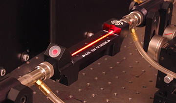
Waveguide at JILA used to convert laser light into laser-like UV beams. [Image: Kapteyn-Murnane Group]
For each sample, the researchers first used an infrared pulse to heat the nickel arrays and generate sound waves that propagated both through the sample and across its surface. They then fired in an extreme ultraviolet pulse just a few picoseconds later and recorded the resulting diffraction pattern using a CCD camera. The idea was to vary the delay between the two pulses and plot the resulting changes in diffraction efficiency. Those changes could be used to calculate the velocity of the sound waves, which in turn yielded values for the film's elastic constants.
Disrupting atomic bonds with hydrogen
Frazer and coworkers used this technique to measure the properties of a dual layer of SiC containing fairly small amounts of hydrogen at two different thicknesses. For a sample with a thickness of 46 nm, they recorded a high Young's modulus and a low Poisson's ratio, showing it to have a network of rigid bonds characteristic of a bulk material. In contrast, when the layers were just 5 nm thick they found the inverse—a low Young's modulus and a high Poisson's ratio, revealing a softer, more incompressible state. In fact, the latter sample was nearly an order of magnitude softer than the former.
That picture changed, however, when the researchers instead investigated single layers of SiOC containing substantial amounts of hydrogen. In this case the material's elastic properties remained unchanged (within the experiment's error bars) for samples of different thicknesses. That, say the researchers, is because the hydrogen breaks enough bonds in the bulk to make the atoms there about as unconnected to one another as those on the surface.
Frazer and colleagues believe that these findings should allow scientists and engineers to optimize the design of very thin, robust films “for a host of nano and quantum technologies.” In particular, they say, the results could confer next-generation electronic devices with faster switching and higher efficiencies.