
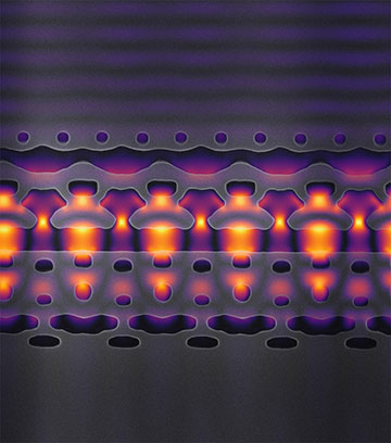
An approximately 5-μm-wide section of an accelerator-on-a-chip. The gray structures focus infrared laser light (shown in yellow and purple) on electrons flowing through the center channel. [Image: Neil Sapra, Stanford University]
Accelerators that use microwaves to boost subatomic particles to nearly light speed usually fill large rooms or even buildings, so researchers must travel to use them. Now scientists at a laboratory of Stanford University, USA, have developed a small, laser-driven linear accelerator integrated onto a silicon wafer (Science, doi: 10.1126/scienceaay5734).
The device imparts up to 0.915 keV of energy to electrons over a distance of just 30 μm, which is equivalent to a gradient of 30.5 MeV per meter. Although this device is still a proof of concept, such chip-sized accelerators could make particle accelerators more accessible to researchers who want to apply them to biomedical and chemical studies.
The design challenge
Accelerators driven by near-infrared laser light instead of radio-frequency waves already exist, but they “require a densely packed optical table to a room's worth of elements to accomplish splitting and phase-control off-chip,” says Neil Sapra, a Stanford graduate student in physics and lead author of the research. With the microscale accelerator, scientists can carry out the splitting and phase control within a waveguide network occupying a tiny sliver of on-chip real estate.
The biggest challenge in the work was designing the integrated photonic structure, according to Stanford electrical engineering professor and OSA Fellow Jelena Vuckovic, who (along with OSA Fellows Robert Byer and Olav Solgaard) led the research team. “Traditional photonics and intuitive solutions didn’t work and wouldn’t provide a sufficient acceleration gradient and efficiency to build an accelerator,” she says. The small features that manipulate the light inside a waveguide to create the particle-accelerating fields also introduce reflections and scattering, Sapra adds.
Instead, the team used a design technique called “inverse photonics,” which computationally searches the full space of possible photonic structures for the shape that optimizes the device’s efficiency and acceleration gradient with minimal damage to the material. The resulting instrument consists of a 500-nm-thick device layer stacked on a 3-μm-thick buried oxide layer, with 30 periods etched over a 30-μm length. The researchers sent an electron beam of 83.4 keV (moving at 51% of light speed) into the waveguide and measured its spectrum with and without illumination from a 1.94-μm-wavelength laser.
“The resulting solution is highly non-intuitive but beats any traditional approaches in performance and can be scaled to a multi-stage accelerator,” Vuckovic says.
Future plans
The prototype by the team at Stanford and the SLAC National Accelerator Laboratory, USA, is part of a larger effort, called the Accelerator on a Chip International Program, to shrink the size of these instruments and increase their portability.
In this work, Sapra says his group demonstrated dielectric laser acceleration over a single stage of acceleration, but they would need around 1,000 of such stages for an on-chip MeV-scale accelerator.
To get the energy gradient up to this range, the researchers will pursue a two-step strategy. First, they will work on improving the system efficiencies of the entire system to increase the amount of acceleration per stage. In addition, the researchers will cascade multiple stages and integrate them in a linear on-chip geometry to reach toward higher particle-beam energies, which could be used someday in medical applications, such as precisely targeted cancer therapy.
“In addition, on-chip particle accelerators provide a table-top solution to X-ray sources for imaging in industry, as well as in biological and materials research,” Sapra says. “Currently, there are only a handful of free-electron laser facilities around the world that researchers compete intensely for ‘beam-time’ on,” says Sapra. “Imagine, in the future, being able to purchase a free-electron laser X-ray source based on an on-chip particle accelerator for an individual lab-space!”