
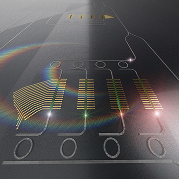
Scientists at George Washington University, USA, have proposed a “photonic tensor core” that can perform computationally intensive matrix multiplications for machine learning using the efficient interaction of light at different wavelengths with multistate photonic phase-change memories. [Image: Mario Miscuglio]
Neural-net computing and machine learning can enable seemingly magical results—from computer face recognition, to on-the-fly image classification, to microsecond translation from Dutch to Mandarin. Under the hood, however, these functions rely largely on grinding through stacks of repeated matrix multiplications, a computationally intense and power-hungry process.
That need has led to a search for specific hardware systems—such as Google’s Tensor Processing Unit (TPU)—that are optimized to handle such high-end number crunching. Two researchers from George Washington University (GWU), USA, have now unveiled the details of a photonic alternative to the TPU: a modular “photonic tensor core” (PTC) that does these matrix calculations entirely in the optical domain (Appl. Phys. Rev., doi: 10.1063/5.0001942).
The GWU team reports that its system can perform two to three orders of magnitude more operations per joule of energy than electronic tensor cores. That advantage, the researchers say, could make it useful as a component of machine-learning systems in applications ranging from data-intensive science to autonomous-vehicle systems to 5G communications.
Big MACs
Recent years have seen a variety of efforts to develop photonic deep neural networks—computing platforms for AI and machine learning that operate optically rather than electronically (see “Optical Neural Networks,” OPN, June 2020). Instead of building a full-fledged photonic neural net, the team behind the recently reported work, GWU scientists Mario Miscuglio and Volker Sorger, focused on how photonics could reduce the computational loads associated with one key function: the multiply–accumulate (MAC) matrix operations that lie at the heart of all neural nets, whether optical or electronic.
The energy and time costs associated with MAC operations in machine learning have already spurred a quest for better electronic systems to handle such math. The best-known example is Google’s TPU, a chip optimized for the linear algebra of AI (and designed to work with Google’s open-source Tensor Flow software library). Initially unveiled in 2016 and since evolved through several generations, the TPU has featured in a number of the company’s more celebrated AI feats, such as the AlphaGo system that was the first computer program to defeat a professional human Go player.
Taking advantage of light’s wave nature
As strong an offering as the TPU is, Miscuglio and Sorger point out that it can still eat up lots of power, and sport relatively long run times, on tasks such as image processing. To get to a potentially better-performing alternative, they looked for an architecture that exploited the wave nature of light. The elements of MAC operations—matrix summation and multiplication—“happen directly” when performed with waves, according to Miscuglio; coherent addition of wave amplitudes allows summation, while interactions of optical waves with matter can execute multiplication. “It’s inherent within the nature of the system.”
The team also sought to eliminate the latencies that plague electronic systems owing to the need to repeatedly transfer data from the processing unit to memory.
“In digital electronics there’s a strong dichotomy between memory and processors,” notes Miscuglio. “In a real [biological] neural network, each neuron can both process and store data. And similarly we do these with the photonic tensor … There won’t be any latency, because everything is happening while the photons are traveling.”
WDM enables parallelism
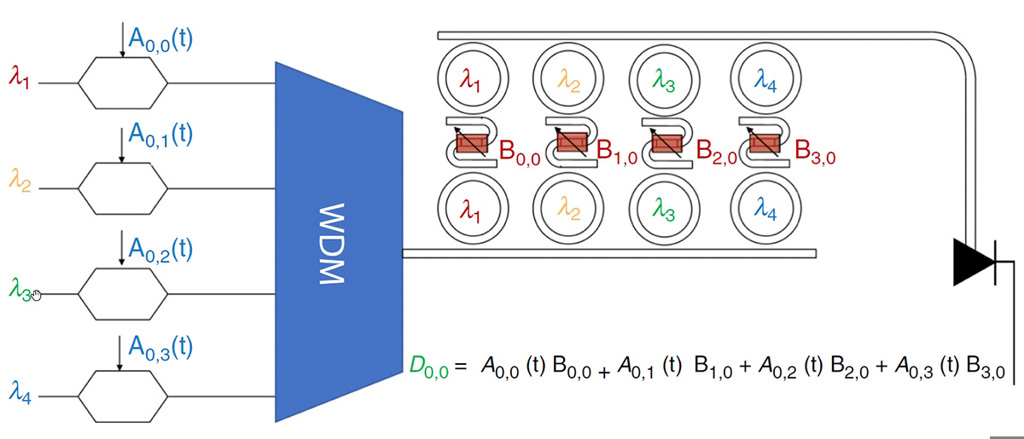
In the PTC, WDM signals enter the waveguide, are spectrally filtered by micro-ring resonators, and interact with weights in a pre-set photonic memory to enable element-wise matrix multiplication. [Image: Reprinted from M. Miscuglio and V.J. Sorger, Appl. Phys. Rev. 7, 031404 (2020), with the permission of AIP Publishing] [Enlarge image]
The specific design that the team developed is for a tensor core unit that can execute a 4×4 matrix multiplication, and that would constitute the building block of a larger processing unit such as a TPU. In their scheme, an optical signal with different wavelength components, each for a different row of the 4×4 matrix, is combined via wavelength-division multiplexing (WDM) to enable parallel processing; this WDM signal then injected into the processor waveguide.
The light signal is then spectrally filtered, by micro-ring resonators, into component wavelengths, which perform the matrix multiplication via light–matter interaction with the weighted columns of the matrix. The weights themselves are realized in a nonvolatile photonic memory implemented directly on the chip. The result of this light–matter interaction is an element-wise multiplication entirely in the optical domain—the scalar result of which is summed at the end of the line using a photodetector.
Phase-change-material memory
A key component of the system is the nonvolatile photonic memory used to set the weights of the matrix columns. For this, Miscuglio and Sorger chose a phase-change material (PCM), Ge2Sb2Se5, whose optical properties vary depending on whether the material is crystalline or amorphous. The PCM is arrayed in 30×250-nm wires, arranged as a grating and tied to tungsten electrodes.
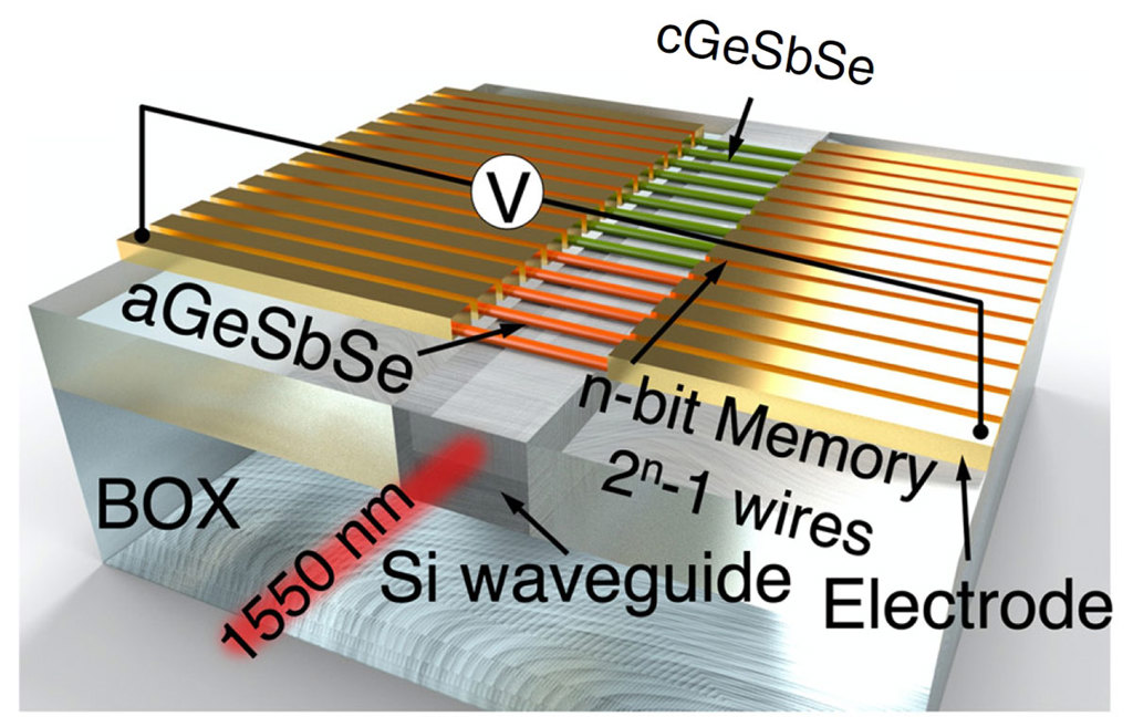
The photonic memory is implemented as nanowires of a phase-change material (PCM) adjacent to the photonic waveguide. During the training of the neural network, the weights of the matrix columns are set by electrothermal heating of the PCM. [Image: Reprinted from M. Miscuglio and V.J. Sorger, Appl. Phys. Rev. 7, 031404 (2020), with the permission of AIP Publishing] [Enlarge image]
During the training of the neural network, electrothermal Joule heating, via the tungsten electrodes, is used to write the desired weights of the matrix columns as local phase changes in the nanowires. In the trained neural network, the weights in the matrix multiplication play out as relative changes in the optical loss, due to these pre-written phase changes, as the optical wave signal interacts with the PCM.
While setting the weights electrothermally in this way does take energy, the team stresses that that energy cost disappears once the network is trained and the weights are set—the actual matrix multiplications of the working neural network are completely optical. “Once it’s written,” says Miscuglio, “you just let the photons flow, and they will do the rest.”
Sorger stresses that the close proximity of the optical signal in the waveguide to the memory in the PCM offers a big speed advantage. “You want the memory very close to where you need it, and in our case it’s almost literally nanometer-close,” he says. “That means that the optical read [time] is literally a few picoseconds.” And, once the network is trained for operation, the static power consumption drops to near zero, owing to the optical nature of the setup.
Wide application space
In light of these power and efficiency advantages, Miscuglio and Sorger see wide range of possible applications for the PTC as a modular component of machine-learning systems. The advantages could be particularly great, they argue, for performing intelligent tasks in which data signals already exist in optical form, such as 5G networks, surveillance systems and sensors. That’s because the PTC would eliminate the need for electro–optical conversions, saving both time and power.
As an example, Miscuglio says, a PTC-enabled system might be used to pre-screen the vast data streams coming from radio astronomy, which are already in transmitted via fiber in the optical domain. The PTC could be used to intelligently discriminate and reduce this firehose of data, cutting down on the volumes that need to be sent on to high-performance electronic supercomputers for more detailed (and power-hungry) processing.
“Electronics is so well established that it’s very hard to compete,” Miscuglio observes. “But you can be complementary.” Sorger adds that the speed advantages could mean there’s a place for the PTCs in other intelligent systems, too—such as “the entire world of autonomous vehicles, where you need to make a decision very fast.”
Thus far, much of the team’s work on PTCs has been numerical, with some experimental testing of components such as the PCM memory. But Sorger says the team has made additional progress toward a prototype full PTC chip that he hopes can be unveiled in the coming months.