
Researchers at the University of Oxford and the University of Warwick, U.K., have demonstrated a method for creating individual, well-ordered diamond nitrogen-vacancy (NV) centers with near-100-percent yield—a potential step toward accelerating the development of some quantum technologies. [Image: Oxford University]
In the continuing quest for a platform for fault-tolerant quantum computing, as well as for quantum memories and quantum repeaters for long-haul communications, many researchers have focused on so-called color centers in diamond—particularly nitrogen-vacancy (NV) centers. But one big hurdle has been creating and organizing these atomic-scale features in a reliable way that allows their position to be nailed down at specific, well-ordered points in the crystal lattice.
Now, a research team headed up by scientists at the University of Oxford, U.K., has devised a method that uses a femtosecond laser pulse to carve out a lattice vacancy, followed by a second pulse train to anneal the defect in place (Optica, doi: 10.1364/OPTICA.6.000662). The result, the researchers say, is a “near-deterministic” method for creating well-ordered arrays of NV centers in diamond with nanometer-scale accuracy.
Qubit candidate
NV centers are negatively-charged defects in the diamond crystal lattice, where a carbon atom is replaced in the crystal unit cell by a nitrogen atom and a lattice vacancy. They’ve attracted particular attention as one of several candidates for a quantum bit (qubit) to undergird fault-tolerant quantum computing. That’s because the spin states of NV centers can have relatively long coherence times—that is, they can hold onto delicate quantum information longer than some other systems. Moreover, the spin-state information can be easily read out from the NV center using optical transitions.
The most common methods for making diamonds with NV centers include ion implantation and electron-beam irradiation, though laser processing has also recently experienced some success. The problem with all of these methods, however, is that they include a global thermal annealing step, in which the vacancy created is allowed to diffuse through the lattice and to bind at random with a nitrogen impurity in the diamond to create the NV center.
As a result of this non-deterministic process, figuring out the position of NV centers in the diamond host has a distinctly probabilistic flavor, with the likelihood of finding a center at a specific site as low as 37 percent. That’s fine for quantum experiments in the lab—but it’s apt to stack up poorly for engineering workable devices for the market.
Local annealing—with feedback
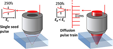
The technique works by irradiating a location in the diamond crystal lattice with a single seed pulse to create a vacancy, and following that with a series of annealing pulses to control diffusion of the vacancy and formation of the NV center. [Image: Y.-C. Chen et al., Optica, doi: 10.1364/OPTICA.6.000662]
To get to a more deterministic approach, the Oxford-led team—headed up by the materials scientist Jason Smith, along with engineering professors Patrick Salter and OSA Fellow Martin Booth—thought locally rather than globally, devising a scheme that made the annealing process much more targeted and carefully controlled.
The team began by obtaining single-crystal diamonds (provided by the De Beers synthetic-diamond subsidiary Element Six) with 1.8-parts-per-million concentrations of nitrogen, but without NV centers. The researchers placed the diamonds on a precision-translation stage that provided 3-D positioning at a 2.5-nm resolution, beneath a 1.4-NA microscope objective.
Next, the team zapped the sample at carefully spaced points with a 29-nJ “seed” pulse from a 790-nm, 250-fs laser, with each pulse creating a lattice vacancy at that point within the diamond. Immediately following the seed pulse, a train of “annealing” pulses, with an energy of 19 nJ and a repetition rate of 1 kHz, zeroed in on the region with the freshly created vacancy, causing the vacancy to diffuse within the diamond crystal lattice.
While the vacancy was diffusing, the team monitored the fluorescence signal coming from the irradiated area. As soon as the fluorescence signaled that the vacancy had “found” a nitrogen atom and created an NV center, the annealing pulse train was switched off, freezing the NV center in place.
A step toward quantum devices?
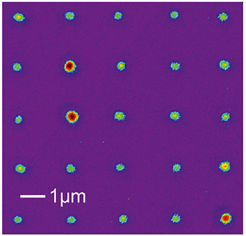
Fluorescence image shows high-yield, 5×5 array of single NV centers on a square grid. [Image: Y.-C. Chen et al., Optica, doi: 10.1364/OPTICA.6.000662]
Using the method, Smith’s team was able to create a rectilinear, well-ordered array of 25 laser-written NV centers, with a positioning accuracy of roughly 33 nm in the image plane—4.5 times smaller than the half-width of the focused laser spot itself. The researchers were also able to characterize the 3-D orientation of each center within the crystal, through polarization readings from fluorescence measurements at those points.
The team believes that development of the technique—which they argue is fast and “straightforward to implement with other aspects of subsurface laser writing in crystals”—could constitute “an important step in developing routes for the manufacturing of devices that use individual color centers as quantum light sources or qubits in quantum technologies.” Co-team leader Martin Booth, in an Oxford press release accompanying the work, called the process “a potential game-changer in the engineering of the required materials.”
“There is still more work to do in optimizing the process,” Booth said. “But hopefully this step will help to accelerate delivery of these technologies.” His colleague Jason Smith suggested in the same release that the ability to deterministically write NV centers in diamond could mark a first step toward devices that could eventually pack “high densities of qubits onto a solid-state chip, which could be entangled with each other using optical methods to form the heart of a quantum computer.”
In addition to researchers at Oxford, the project included scientists from the University of Warwick, U.K.