
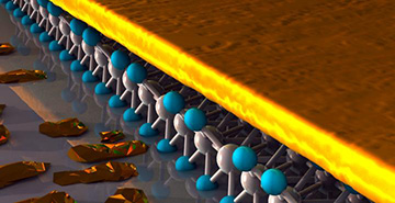
Researchers from the Moscow Institute of Physics and Technology (MIPT) have created smooth, transparent and conductive films of gold less than 10 nm thick by depositing the gold on a 2-D layer of MoS2. The thin gold films could serve as transparent electrodes in future applications such as ultrathin photovoltaic films, flexible displays and devices, and more. [Image: Ella Maru Studio]
The ongoing drive for thinner and thinner optoelectronic devices has boosted interest in ultrathin metal films—especially sub-10-nm-thick gold—that can act as transparent electrodes. But getting gold to such wispy thicknesses, and making the resulting ultrathin film uniform and continuous, has proved a tough trick.
A research team at the Moscow Institute of Physics and Technology (MIPT) has now unveiled a technique for creating continuous, conductive and transparent films of gold as little as 3 to 4 nm thick (Adv. Mater. Interf., doi: 10.1002/admi.201900196). The secret lies in using another ultrathin material—monolayer, 2-D molybdenum disulfide (MoS2)—as a go-between to connect the gold film to the underlying substrate. The researchers believe that their technique opens opportunities for a new science of “quasi-2-D” metals.
The 10-nm conundrum
Gold is a particularly good candidate for plasmonic and optoelectronic applications, owing to its low optical losses in the visible and near-IR bands relative to some other metals. As a result, thin gold films already find use in photonic and plasmonic devices, as well as in plasmonic waveguides and some exotic metamaterials. And engineers and designers are eager to put the potential advantages of still thinner, transparent, ultrathin gold to work as an electrode material in thin-film photovoltaics, LEDs, photodetectors, and super-slim, flexible touchscreens and displays.
Such applications, however, require the gold to be, figuratively speaking, hammered down to thicknesses of less than 10 nm. And the chemistry of gold has been notoriously uncooperative in that effort.
The most common technique for obtaining thin gold films, thermal evaporation followed by deposition, has been able to achieve uniform, homogeneous films with a thickness of 20 nm or so. But efforts to deposit films thinner than that, and particularly below the 10-nm threshold for optical transparency, have run up against gold’s poor “wetting”—its underwhelming ability to maintain contact—with typical optoelectronic substrates like silicon oxides and glass. The result has been patchy, inhomogeneous films unsuitable for cutting-edge applications.
MoS2 as a go-between
One approach to overcoming these problems would be adding another ultrathin material to act as an adhesion layer between the substrate and the gold. A natural candidate would seem to be graphene, the monolayer sheets of carbon atoms whose discovery a decade and a half ago kicked off broader interest in 2-D materials. But gold turns out to have poor wetting properties with graphene, too, with the metal piling up on the 2-D carbon in vertical pillars rather than continuous sheets.
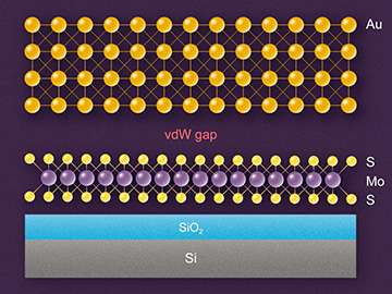
The MIPT technique deposits a monolayer of MoS2 atop a silicon wafer/SiO2 substrate. The MoS2 acts as an adhesion layer—a go-between that allows uniform deposition of the gold on the substrate, separated by a “van der Waals (vdW) gap.” [Image: MIPT Press Office]
The MIPT team—led by Valentyn Volkov, also affiliated with the University of Denmark—saw better prospects in another up-and-coming 2-D material, monolayer MoS2. One of a class of materials called transition-metal dichalcogenides (TMDs)—of considerable interest as possible semiconductor layers in optoelectronic applications (see “Optolectronics in Flatland,” OPN, July/August 2015)—MoS2 struck the MIPT scientists as a particularly good bet as an adhesion layer for ultrathin gold. That’s because gold, while a “noble metal” that generally shows little interest in bonding to other elements, does have a known affinity for stable bonds with sulfur.
Dramatically improved nanolayers
To test out the idea, the team used chemical vapor deposition to coat several silicon wafers (which had been pre-coated with a 285-nm-thick SiO2 layer) with continuous, single-layer or 2-D MoS2. Then, they used an electron-beam evaporator to lay down gold films of different thicknesses atop the MoS2 monolayers. Scanning electron microscopy (SEM) revealed that the gold grown on the 2-D MoS2 layers showed dramatically improved uniformity and continuity, with an almost continuous nanostructure down to thicknesses of around 4 nm.
The researchers also used spectroscopic ellipsometry to investigate the optical properties and dielectric functions of the ultrathin films, and also measured the electrical sheet resistance of the films. They found that, while the resistance and optical losses tended to increase as the film got thinner, the gold remained conductive down to a thickness of 3 to 4 nm.
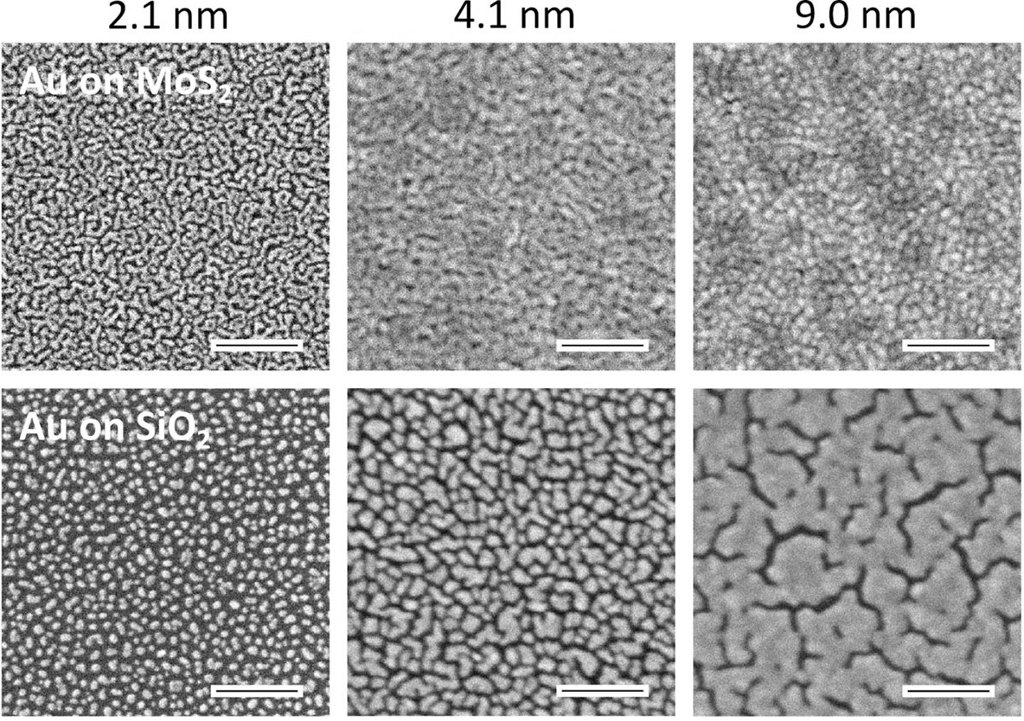
SEM images of the gold films of thicknesses between 2 and 9 nm deposited on the MoS2 intermediate adhesion layer (top row) show far greater uniformity and few gaps compared with comparable films deposited directly on a silicon dioxide substrate (bottom row). Scale bar: 100 nm. [Image: courtesy of Yury Stebunov et al.] [Enlarge image]
An emerging quasi-2-D-metal science?
With thicknesses exceeding 3 nm, the gold layers achieved by the MIPT team are far from true 2-D materials such as graphene and MoS2, which consist of only a single layer of atoms or molecules. Nonetheless, in a press release accompanying the research, one of the study coauthors, OSA member Aleksey Arsenin, characterized the group’s research as “merely the beginning of quasi-2D metal science.”
In particular, the researchers point out in the paper that, while demonstrated in this study with gold and MoS2, the group’s techniques could, in principle, be used to fashion ultrathin metal layers with other combinations of metals and TMDs. And research team leader Volkov stresses that the team’s effort to characterize the film’s optical and electrical properties should pay dividends in the design of new applications. “Any researcher can use our data to model photonic or optoelectronic devices or even the artificial materials also known as metamaterials,” he said.
“A while ago, these materials were inaccessible even to scientists,” Arsenin observed. “With our technology, we can talk about the prospects they hold for flexible and transparent electronics. Hopefully, we will soon see it in production.”