
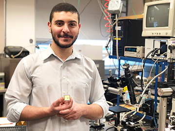
OSA Student Member Hossam Shoman was part of a team that developed a low-footprint system for controlling micro-ring resonators on silicon photonic chips. The team believes that the advance will improve the prospects for leveraging large arrays of ring resonators in real-world integrated photonic applications. [Image: University of British Columbia]
Much of integrated silicon photonics boils down to the cutthroat competition for scarce chip real estate. In that contest, ring resonators, with their compact form factor, would seem to have a significant edge.
But the accompanying components for monitoring and controlling those tiny rings—photodetectors for keeping tabs on the actual resonance, and heaters for phase-shift tuning of the rings as needed—can be space hogs on the chip. The need to include those components has thus far held back realizing some of the big dreams being spun for ring resonators as a linchpin of silicon photonics.
Now, a research team at the University of British Columbia (UBC), Canada, has fine-tuned a doped silicon nanowire waveguide to operate as a highly efficient control element that sits right in the resonator, and has demonstrated the ability of such elements to control a 16×16-resonator switch (Optica, doi: 10.1364/OPTICA.6.000084). The researchers believe that the system—which, they stress, requires “zero change” to existing silicon chip foundry fabrication processes—could mark out a path for making the promising ring resonator systems of recent lab demos practical on real-world chips.
Making ring resonators foundry-friendly
Micro-ring resonators, with diameters as small as tens of microns, have cropped up as a key design element in applications ranging from biosensors to communications and quantum computing. To realize their potential, however, the tiny rings need to be monitored and controlled, not only to allow on-the-fly reprogramming for certain functionalities, but to tune the rings’ resonances to compensate for inevitable fabrication imperfections and temperature variations.
That usually involves additional optical and thermo-electro-optic components, to monitor each ring’s resonance properties and adjust them in a continual feedback loop. Quite apart from taking up space on the chip, those components can require additional processing steps, making their setup unfriendly to current chip foundries.
To get past that problem, the UBC team, which included OSA Life Member Lukas Chrostowski and OSA Student Member Hossam Shoman, looked at the potential for a silicon nanowire—an eminently foundry-friendly element—to act as both a monitor and a controller for ring resonators. In work published a few years ago, several members of the team had already demonstrated the use of such nanowires as photconductive heaters to tune and stabilize wavelengths in a paired-microring system.
Doping holds the key
Scaling up that system to a larger on-chip resonator array, however, required knowing more about the actual quantum efficiency and dynamic range of the nanowires. The team has now done that homework, and demonstrated that the nanowires appear to have what it takes to control significant arrays of resonators in several real-world configurations.
One key to the nanowire waveguides’ ability to both monitor and control the rings is the doping of the waveguide core. Specifically, the team used n-type doping of the core, with the percentage of doping carefully tweaked to be low enough to allow low-loss light propagation, but high enough to let the waveguides serve a double function as both micro-ring monitor and controller.
Specifically, the doping allows the waveguides to provide measurable, micro-ampere photocurrents, with quantum efficiencies (QE) approaching 200 for low input optical power levels. That lets the wires potentially act as tiny, precise power monitors in the optical circuit, and to use the photocurrent to report back on the optical resonance conditions in the ring. Meanwhile, the doping also fine-tunes the nanowire resistance such that, with the application of a CMOS-compatible voltage bias, the device can function as a tiny photoconductive heater to allow thermo-optic tuning of the resonator.
Controlling a 16×16 array
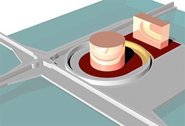
Illustration of a photoconductive heater (gold area of ring) integrated into a ring resonator with an 8-μm radius. [Image: H. Jayatilleka et al., Optica, doi: 10.1364/OPTICA.6.000084]
After detailed tests to measure the nanowire QE and other properties, the team built several prototypes involving arrays of resonators with integrated nanowire photoconductive heaters. One was a 16×16-resonator switch, occupying a total area of only 6.1 mm2. The team was able to tune and program the switch to automatically align the resonances of the 31 rings along the longest path in the array (the diagonal). The team also tested out a 14-ring coupled-resonator optical waveguide (CROW), a potentially attractive configuration for optical filters, delay lines and other applications.
The demonstrations constitute, according to the team, “the largest, yet most compact, automatically controlled silicon ring resonator circuits to date.” Interestingly, the feedback loop for controlling each ring is local to the ring itself, and reacts to local conditions and to heat leaking over from the ring’s nearest neighbors. That, according to the team, makes the approach “readily scaled to systems with any number of rings, as long as there is sufficient light inside the rings for accurately sensing their resonance conditions.”
Reduced footprint
The researchers have a few improvements to make to the system. One lies in the power required for tuning—48 mW per ring resonator in the devices used in the 16×16-resonator switch, across a free spectral range of 12.1 nm. The team believes that that power need can be hammered down by an order of magnitude by fine-tuning the silicon substrate. The nanowire doping also leads to relatively high insertion losses at the grating connection with the light source; here again, the team believes that future design improvements can mitigate those losses.
Shoman, the grad student who worked on the research team, is enthused about the prospects of the technology to lead to smaller chips that could benefit the biomedical-sensing application space in particular. “This will reduce the footprint compared to other devices, and allow for large scaling of photonic systems,” he noted in a UBC press release.
“We’re working on integrating and packaging the chips in cost-effective ways for consumers and countries that can’t afford medical equipment,” Shoman said. “Imagine a sensor on the back of your phone that could detect your blood sugar level.”