

A U.C. Berkeley-led team has devised a low-optical-loss method for creating a chip containing more than 50,000 optical switches. [Image: Younghee Lee graphic]
As the world’s appetite for massive internet data flows continues to expand, data centers have increasingly looked for salvation toward replacing electronic switches with optical ones. Such switches promise to dramatically cut back on energy costs, helping to make the ever-increasing demand growth manageable.
But even as engineers have sought creative ways to pack more and more components onto silicon-based photonic integrated circuits (PICs), they confront a pesky limitation: the maximum die size at the silicon chip foundry, imposed by the 2-to-3-cm dimensions of the “reticle” or photolithography mask. One option for building bigger optical switches is to “stitch” together smaller, reticle-limited switch blocks into a larger array. But it’s been tough to stitch a larger chip together in this way without unacceptably high optical losses.
Now, researchers headed up by OSA Fellow Ming C. Wu of the University of California, Berkeley, USA, believe that they’ve found a way around that quandary (Optica, doi: 10.1364/OPTICA.6.000490). By tapping earlier work by the same group toward a very-low-loss, microelectromechanical-system (MEMS) switching architecture, and by carefully tapering waveguides at stitching points between reticle-limited switch blocks to dramatically cut optical losses, the team has fabricated what it believes is “the largest integrated photonic switch ever reported.”
A “freeway overpass” switching model
As is well known, one of the driving forces for silicon photonic integration is the ability to plug into the well-developed, low-cost manufacturing processes honed over decades for CMOS chips. And, as with electronic chips, much of the action in PICs has involved cramming greater and greater concentrations of photonic components onto smaller and smaller spaces. But switches built using arrays of Mach-Zehnder interferometers or microring resonators have often logged high cumulative optical losses, diminishing their effectiveness.
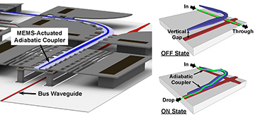
In the team’s switch architecture, a MEMS-activated coupler, upon a voltage bias, shunts optical data to a new path using a second level, much like a freeway offramp or overpass. [Image: T.J. Seok et al., Optica, doi: 10.1364/OPTICA.3.000064 (2016)] [Enlarge image]
Several years ago, Wu’s team demonstrated a novel switch design built on a very different premise: a two-layer waveguide design, with switching empowered by MEMS-actuated, vertical adiabatic couplers between the layers (Optica, doi: 10.1364/OPTICA.3.000064). In the switch’s “off” state, data transits unimpeded through waveguides in the lower layer. When a voltage bias changes the switch to the “on” state, the MEMS-based coupler electrostatically closes the gap between the upper and lower waveguides, shunting the optical data onto a new path much like a freeway onramp or overpass—with extremely low optical losses.
Stitching switch blocks together
Wu’s team has been able to create switch block arrays as dense as 128×128 switches on a single, 1.6×1.7-cm die. But that work took the researchers close to the limit imposed by the photomask or reticle size in CMOS manufacturing. To build a bigger array, they sought an effective way to stitch individual switch blocks together.
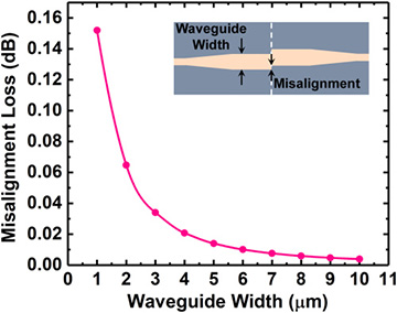
The team found that “stitching losses” caused by misalignments between individual switch blocks would dramatically decrease if the waveguides joining the blocks were tapered open. [Image: T.J. Seok et al., Optica, doi: 10.1364/OPTICA.6.000490 (2019)]
To do so, the team looked in detail at the sources of optical loss when waveguides emerging from different switch blocks are stitched together. The team found that even tiny, 100-nm misalignments between sub-micrometer waveguides stitched together between switch blocks can produce heavy optical losses, on the order of 0.1 dB for linking waveguides 1 μm wide. More important, the team’s calculations suggested that tapering open the waveguide to a 10-micron width at the point of connection could dramatically reduce the stitching loss, to less than 0.004 dB per waveguide.
One chip, >50,000 switches
Wu’s team rolled these ideas up into a prototype array of nine 80×80-switch blocks, stitched together in a 3×3-block array, to create a 240×240 array embedding more than 50,000 switches on a single 4×4-cm chip. The proof-of-concept chip sported switching times of less than 400 ns. The maximum on-chip loss on the longest possible optical path was a moderate 9.8 dB, but the team believes that that number can come down substantially with further improvements in the switching architecture—allowing scaling to still higher numbers of switches per chip.
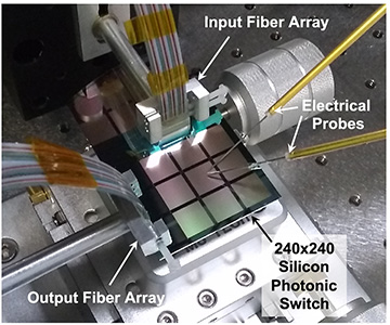
The team’s proof of concept stitched together nine 80×80-switch blocks in a 80×80 array. [Image: T.J. Seok et al., Optica, doi: 10.1364/OPTICA.6.000490 (2019)]
Wu believes that the ability to go beyond the die limit, and to create switches with rapid switching times, could “enable new functions in data center networks,” according to a press release that accompanied the new research. “Larger switches that use bulk optics are commercially available, but they are very slow, so they are usable in a network that you don't change too frequently,” he says. “Now, computers work very fast, so if you want to keep up with the computer speed, you need much faster switch response.”
The team is currently at work on refining the manufacturing process to create even larger, lower-loss switches.