
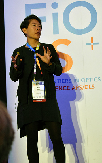
Teri Odom at FiO+LS
One of the four core themes of this year’s Frontiers in Optics/Laser Science meeting in Washington, D.C., is nanophotonics and plasmonics. A Visionary Speaker talk on Monday by materials scientist Teri Odom of Northwestern University, USA, kicked off that theme in memorable style, with a talk on the frontiers in nano-optics titled “Peering Through the Looking Glass.”
It’s all about structure
Odom suggested that, in thinking about what can be done with nanoscale, subwavelength optics, three basic types of materials—metals, dielectrics and semiconductors—constitute a sort of palette for a variety of optical effects. “Sometimes you’d like perfect reflection,” she said, “sometimes perfect transmission, sometimes you’d like to have anomalous reflection and transmission.” Accomplishing those effects involves laying out carefully selected combinations of materials in finely engineered arrays of nanoresonators.
“Structure is the key parameter,” Odom said. “You can combine all three materials at different length scales for interesting applications.”
From Huygens to metasurfaces
The notion that you can use tiny scatterers to engineer wavefronts “is actually 350 years old,” dating back to Christiaan Huygens, Odom noted. Today, this notion plays out in the area of metasurfaces, 2-D surfaces of nanoscale antennas, in orderly arrangements that, according to analytical wave-optics equations, will shift phase by a specific amount. These arrays can give rise to effects like anomalous reflection and optical vortices—while also offering the potential to dramatically scale down device sizes, and pack the functionality of multiple optical elements into a single, tiny device.
Odom touched on a number of recent advances in using dielectric materials in particular to advance nano-optics. These include the CMOS-compatible, high-efficiency flat “metalenses” coming out of the lab of Federico Capasso at Harvard University; silicon-based metasurfaces from the group of Yuri Kivshar and others at the Australian National University, which could find use in applications such as “molecular barcoding”; and new nano-optics-enabled approaches to lasers, including the “topological lasing” demonstrated by Boubacar Kanté of the University of California, San Diego. In all cases, said Odom, “the structuring is really the driver to make these applications.”
Plasmonic advantages
While duly acknowledging the fantastic recent work with dielectric metasurfaces, Odom stressed that there’s still plenty of action in the field she’s most associated with—plasmonics, which involves the use of subwavelength metallic nanoparticles to concentrate and scatter light. Plasmonics is often viewed as being at a disadvantage, owing to the big optical losses that metals are susceptible to. But, says Odom, it depends on the application.
“If you compete head to head” between metals and dielectrics in some of these ultraminiaturized devices, she admitted, “metals are going to lose” because of their optical-loss characteristics. But “we’re not interested only in miniaturization,” she maintained. “Metals have interesting properties, and can do things that dielectrics can’t.” One example is the creation of optics that are not just flat, but flexible. “Some of the dielectric systems are impressive,” said Odom, “but tolerances aren’t such that you can integrate them into flexible substrates.”
Flexible and tunable nanolasers
Odom reviewed how some of this is playing out in the work her group is doing in two areas: laser components and lenses. The work starts with the principle of putting metallic nanoparticles—with dimensions on the order of 50 nm—into an array, at diffraction-based spacing, which creates strong dipolar interactions.
By manipulating plasmon lifetime via different particle sizes and configurations, Odom said, “you can take advantage of interesting effects. You don’t have to do anything special except put them into an array to get narrow linewidths.” Moreover, her group’s work has shown that, by changing the refractive-index environment of material that the metallic nanoparticles are situated in, you can shift their resonance wavelengths. And the array structure can, with suitable engineering, achieve the directionality required in a laser.
Odom’s group has demonstrated these principles in a variety of plasmonic nanolasers that use dyes sandwiched in a glass-nanoparticle array as the gain medium. The team has also created switchable dual-mode lasers, with elliptical metallic scatterers in rectangular arrays, which allow different lasing modes to be excited depending on the polarization of the pump light.
In one particularly memorable example she showed, the plasmonic nanolaser is integrated into a microfluidic channel; the device toggles between different lasing wavelengths depending on whether fluid or an air bubble is being pumped through the channel. And her team has fashioned stretchable plasmonic nanolasers, on an elastomer substrate, that use out-of-plane, quadrupole lasing modes to provide highly directional laser light—the wavelength of which changes when the substrate is stretched.
Small particles, big frontiers
On the lens front, Odom’s group has created processes that, she said, use nanoparticles as localized “building blocks” whose organization is tuned to specific optical properties using genetic algorithms. The result is systems whose resolution and focal length can be tuned on the fly by simply “stamping” predesigned masks onto the substrate.
In the end, said Odom, all of these techniques rely on leveraging “a mixture of materials, and the ability to structure them for the nanoscale to the microscale and beyond.” Within those tiny length scales, she concluded, “the frontier is pretty big.”