
![]()
The Harvard–Nokia Bell Labs work has downsized the technology embodied in conventional lithium niobate (LN) electro-optical modulators (right) to a chip-scale device (center) that reportedly is 20 times more efficient. [Image: Harvard SEAS]
Electro-optic modulators, which convert electronic data to optical signals, are key components of long-haul telecom networks—and, for decades, lithium niobate (LN) modulators have constituted the workhorse technology. But these bulky, power-hungry devices have proved resistant to chip-scale integration. That has represented a stumbling block in the drive toward low-power, ultra-low-loss photonic circuits, not only for next-gen telecommunications but also for data-intensive conventional computing and quantum information processing.
Now, a research team led by OSA Fellows Marko Lončar of Harvard University and Peter Winzer of Nokia Bell Labs has devised a way to radically shrink both the size and the driving voltage of LN modulators (Nature, doi: 10.1038/s41586-018-0551-y). The result is a device 100 times smaller and 20 times more efficient than existing modulators—and one that’s poised for on-chip integration. The researchers envision a vast application space for the new modulators, both in high-bandwidth data communications and in reconfigurable optical circuits for other areas, ranging from microwave signal processing to photonic neural-network computing.
Voltage problems
Over the years, LN modulators have gotten the nod owing to the excellent electro-optical properties of lithium niobate. In particular, the symmetry characteristics in LN crystals leads to a strong Pockels effect (that is, to changes in the material’s optical properties in response to an applied electric field). Those material properties, in turn, mean that tiny applied voltage changes can alter the crystals’ refractive index, on ultrafast, femtosecond timescales.
The problem comes when you try to scale down the fountain-pen-sized LN modulators common in existing telecom networks into something that can fit on a chip. Because of fundamental challenges in etching waveguides into lithium niobate, current-generation NB modulators must rely on waveguides with relatively large mode sizes and poor light confinement. That shortcoming, which in turn imposes limitations on other design details, forces the modulators to operate at drive voltages of 3 to 5 V—well beyond the roughly 1-V levels required to play well with typical CMOS circuitry.
As a result, LN modulators have required electrical amplifiers that have kept their size and power consumption large—and researchers have looked to other materials, including silicon, indium phosphide, polymers and plamsonic surfaces, to develop chip-scale modulators. Unfortunately, none of these alternatives has put together the compelling package of electro-optic properties sported by LN modulators.
Etching LN waveguides
The team behind the new work decided to take another crack at fashioning a chip-scale LN modulator. To do so, they drew on previous work in Lončar’s lab that took a fundamentally different approach to etching in lithium niobate (Optica, doi: 10.1364/OPTICA.4.001536).
In that previous work—which also involved the two co-lead authors of the current study, Cheng Wang (now at the City University of Hong Kong) and Mian Zhang—the team used a technique that involved laying down a single-crystal, 600-nm-thick thin LN film atop a CMOS-compatible insulating layer of SiO2 on silicon. That easier-to-etch material combination, plus tweaks to optimize standard plasma etching processes, allowed the team to dry-etch low-loss LN subwavelength waveguides and fashion them into high-quality microring resonators.
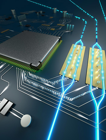
The integrated modulator consists of lithium niobate (LN) waveguides in a Mach-Zehnder interferometer configuration. As electronic data flows into the modulator, changes in the surrounding electric field are converted to changes in refractive index in the waveguides due to LN’s strong Pockels effect, allowing an electronic data signal to be converted to an optical one. [Image: Courtesy of Second Bay Studios/Harvard SEAS]
For the new study, the team applied the same technique to creating integrated modulators in a traveling-wave Mach-Zehnder interferometer configuration, with LN waveguides acting as the interferometer arms. The waveguides run through dielectric gaps that, on an applied voltage, impose a microwave electric field of opposite sign on the two interferometer arms. That field, through the Pockels effect in the lithium niobate, changes the optical phase in the two interferometer arms in an opposite sense—allowing the electrical voltage signal to be changed into an optical one.
“Smaller, faster and better”
Through their improved approach to etching lithium niobate, the researchers found that they were able to create a modulator only 1 cm long and 0.5 cm wide—100 times smaller than conventional LN modulators. The modulator required a driving voltage of only 1.4 V, within the range that it could be directly driven by a CMOS circuit, without bulky amplifiers. And the devices can support data transmission rates of up to 210 Gbit/s—with rates as high as a blistering 1 Tbit/s a distinct possibility with more advanced modulator designs. “It’s like Antman,” co-lead author Wang said in a press release. “Smaller, faster and better.”
A key advantage of the new modulator, according to Peter Winzer, is that it will speed up progress toward moving optics and electronics closer on a single chip—“paving the way toward future fiber-in, fiber-out opto-electronic processing engines,” he said. The result could be a variety of fast, low-loss photonic circuits and applications.
In a particularly intriguing note, the study concludes that the device’s advantages of low optical losses, good electro-optical response, integration and scalability could combine to help create “a new generation of active integrated optoelectronic circuits that can be reconfigured on a picosecond timescale using attojoules of electrical energy.” The team believes those circuits could find use in microwave photonics, quantum networks, topological photonic circuits and photonic neural networks, among other areas.
The prospects have not been lost on Harvard’s Office of Technology Development—which, with Lončar’s lab, has created a start-up company, HyperLight, to “commercialize a portfolio of foundational intellectual property related to this work.”