
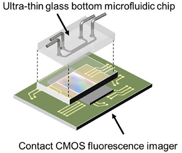
A diagram of the on-chip fluorescence imaging platform showing how the ultra-thin glass bottom microfluidic chip sits on top of the contact CMOS fluorescence imager. [Image: Takehara et al./University of Tokyo]
Researchers from the Nara Institute of Science and Technology and the University of Tokyo, Japan, have combined contact (lens-free) fluorescence microscopy and disposable microfluidic chips to create a new on-chip cell analysis platform (AIP Adv., doi: 10.1063/1.4986872). The platform consists of a complimentary metal-oxide semiconductor (CMOS) fluorescence imager and an ultra-thin glass-bottom microfluidic chip. Proof-of-concept experiments using fluorescently tagged live cells showed that the platform could be used to rapidly image cells grown inside the device with minimal distortion.
A multi-layered imaging platform
According to the new study’s authors, recent advances in semiconductor image-sensor technology, which have given rise to the CMOS chips used in their platform, are driving the development of on-chip, lens-free imaging methods. These methods are especially attractive for automated systems, such as high-throughput biological and medical screening, because they are faster, less expensive and require less human labor than traditional tabletop fluorescence microscopes.
The new cell analysis platform consists of a contact CMOS fluorescence imager paired with an ultra-thin glass-bottom microfluidic chip. The CMOS imager itself has three components: a 120×268-px CMOS image-sensor chip; a thin-film absorption filter for removing excitation light for fluorescent imaging; and a 400-µm-thick fiber optic plate (FOP) that protects the fragile absorption filter from the microfluidic chip that sits on top of it—i.e., the point of “contact” in the contact microscopy platform.
The microfluidic chip has a 10-µm-thick glass base and is topped with a poly(dimethylpolysiloxane) (PDMS) layer threaded with two microchannels. Each microchannel has an inlet and outlet port for introducing cells for imaging, as well as culture media and chemical compounds. The tight, flat fit between the FOP and the glass bottom of the microfluidic chip is integral to maintaining fluorescence-signal intensity and for obtaining high-resolution images.
Team lead Hiroaki Takehara and his colleagues from the Nara Institute used fluorescent 10-µm microspheres to conduct imaging tests on the platform. The resulting images were uniform in resolution, which confirmed for the researchers that the platform was ready for proof-of-concept testing.
Proof-of-concept experiment
To demonstrate the new platform, the researchers placed live endothelial cells with fluorescently dyed nuclei in the chip’s microchannels. In half of the chips, they applied epidermal growth factor (EGF) to the cells via the inlet ports, causing the cells to multiply. When they compared the fluorescence signals between the chips with EGF-treated cells and chips with untreated cells, the chips with the EGF-treated cells gave off a much stronger signal, an indication that the platform is able to detect cell growth.
During the proof-of-concept experiments, the researchers say they were able to achieve images with a spatial resolution of 20 µm. While the image quality isn’t on par with standard fluorescence microscopes, the team says its platform offers “the advantage of being compatible with fully automated systems.” The researchers also suggest that the platform’s small footprint, low price-point and disposable chips could make it of interest to medical professionals for use in implantable devices for measuring glucose and brain activity, as well as to the pharmaceutical industry for developing and screening new drugs.