
Photomicrograph of a part of the QCD array. Each pixel is approximately 109 μm square. [Image: Andreas Harrer]
Designing energy- and cost-effective portable detectors in the mid-infrared (MIR)—ones that avoid thermal noise without bulky or expensive cooling schemes—has been a tough problem. A team of researchers from Austria, Switzerland and Germany reportedly has taken a step toward solving it, with a new design for a quantum cascade detector (QCD) organized into a focal plane array (FPA).
The group’s compact, 64-pixel prototype array provided a strong room-temperature response in the 4.3-μm CO2 absorption band—and should, according to the study, be easily scalable to larger pixel counts. That could, according to the researchers, make the technology a suitable platform for high-resolution, portable infrared imaging applications (Opt. Express, doi: 10.1364/OE.24.017041).
Advantages of QCDs
Designing an FPA-based detector for the MIR has lately been an area of active research, as such array-based detectors have potential applications in thermal imaging, remote sensing and a variety of other applications. Most approaches, however, have had one sort of drawback or another. Some, such as HgCdTe arrays grown on silicon, have proved finicky regarding material and substrate composition, and thus difficult to scale to batch production. Others, such as quantum-well infrared photodetector (QWIP) FPAs, must be cooled to low temperatures, making them difficult to use in portable applications.
Quantum cascade detectors (QCDs) offer a potential way out of this quandary. Their lower thermal load and absence of dark current relative to QWIPs hold out the prospect for room-temperature operation and, thus, better portability. Also, QCD manufacture is compatible with standard indium phosphate (InP) fabrication techniques. And the parameters, such as wavelength sensitivity, can be tuned by adjusting the barrier and well dimensions in the device through well-established methods.
Creating a practical QCD-based FPA does have a stumbling block, however: a trade-off between responsivity and device resistance. As temperature rises, resistance tends to go down. And that, in turn, limits the device’s responsivity at higher temperatures.
Maintaining resistance
The research team, led by Andreas Harrer at TU Wien in Vienna, Austria, set out to design and build a compact QCD FPA that could overcome these issues. Their proof-of-concept is an 8×8-pixel array of semiconductor heterostructures, with each pixel measuring out at 109×109-μm.
Within the heterostructures, the transition energies between quantum wells were carefully tweaked to avoid “back-filling” of lower energy levels by thermally excited carriers. This optimizes the device resistance across temperature ranges, allowing a better extraction efficiency for excited electrons and preventing degradation of responsivity as the ambient temperature increases. Finally, the array is bonded to a CMOS readout integrated circuit, and a gold diffraction grating, processed into the top layer, serves to couple light to the device’s active region.
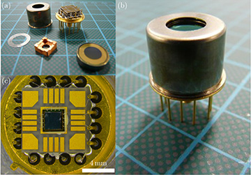
The prototype, including cap, thermo-electric cooler, and the CMOS IC with the QCD array (top and bottom left), is packaged into a compact, 16-pin TO-8 configuration (right). [Image: A. Harrer et al., Opt. Express, doi: 10.1364/OE.24.017041]
The researchers tested the 64-pixel prototype—packaged into a compact, 16-pin TO-8 housing with integrated thermo-electric cooling and a copper cold shield—and found that it delivered single-pixel responsivity of 16 mA/W at room temperature, with “an overall performance increase” relative to previous similar devices in the 4.3-μm wavelength area. And, Harrer noted in a press release, the fabrication scheme—based on molecular beam epitaxy and other standard CMOS techniques—should be easily scalable to larger arrays and smaller pixel sizes. That, he says, “is essential to achieve cost-effective, high-resolution imaging devices in the future.”