
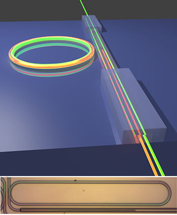
(Top) Artist’s rendering of the zone of coupling between a diamond waveguide and the racetrack microresonator. Pump photons (green), entering the microcavity, undergo stimulated Raman scattering and amplification, enabling lasing at the longer Stokes wavelength (orange). (Bottom) Photomicrograph of racetrack microresonator; path length (600 μm) and bending radius (20 μm) are tuned to make cavity resonant with pump and Stokes wavelengths. [Image: OSA; Optica, doi: 10.1364/OPTICA.2.000924]
Researchers from Harvard University, the University of California, Berkeley, and the Schumberger-Doll Research Center have designed and built an on-chip diamond Raman laser operating in the highly sought 2-micron wavelength area (Optica, doi: 10.1364/OPTICA.2.000924). While the device, relying on an ingenious, racetrack-shaped microresonator, constitutes a proof-of-principle only, the team believes that as the kinks are ironed out, the technology could emerge as a flexible platform for integrated, on-chip Raman lasers operating over a wide spectrum.
The lure of chip-scale Raman
Chip-based Raman lasers have been a perennial quest, with potential applications in spectroscopy, compact sensors and telecom. But although Raman lasers pumped at telecommunications wavelengths have been demonstrated in silicon, the results have been disappointing, owing to silicon’s limited transparency across many wavelengths, its relatively low Raman frequency shift—the crux of Raman’s usefulness in many applications—and poor thermal management outside of a narrow operating window.
Diamond—which can now be fabricated at low cost, and which sports giant Raman shifts, high transparency and Raman gain, and excellent thermal conductivity for high-power operation—has emerged as a great platform for Raman lasers (see “Diamond Raman Lasers,” OPN, September 2014). The trick, however, has been achieving continuous-wave (CW) operation, and integrating these lasers at the chip scale. Thus far, diamond Raman laser demonstrations have typically operated in pulsed mode, and in macroscopic, bulk cavity systems.
Building a racetrack
To move toward an on-chip diamond Raman laser, the research team built on a technique that had previously been used to create a silicon-based Raman laser—an elongated, oval “racetrack” microresonator. The diamond racetrack, coupled to a bus diamond waveguide that can support both the pump and Stokes wavelengths, acts as a high-Q ring cavity in which stimulated Raman scattering and resonant amplification enable lasing at the Stokes wavelength. In particular, the oval is designed to be resonant with both the pump wavelength and the longer wavelength of the scattered Stokes photons, creating a double-resonant amplifying cavity to lower the threshold power for lasing.
Using a device with such a geometry, and pumping at telecom wavelengths, the team achieved CW lasing at around 2 μm, with pump power of only around 85 mW—lower than previous diamond Raman laser demonstrations, according to the team, by a few orders of magnitude. The researchers also believe there’s much room for improvement in the device, through better coupling between the bus waveguide and the racetrack and more careful tuning of the diamond’s crystal structure orientation to the light polarization direction.
Nonetheless, the team argues that the current device—which can be built using standard nanofabrication techniques—“already offers a large amount of flexibility,” particularly through the use of different pump wavelengths and refined resonator geometries. The result, in the researchers’ view, could be a platform for a wide range of optoelectronic applications, at a wide range of output wavelengths.