
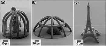
Figures with near diffraction-limited features using dip-in direct laser writing at 405 nm excitation wavelength. Credit: Mueller / KIT
Building on advanced optical lithography techniques, German researchers at the Institute of Nanotechnology at the Karlsruhe Institute of Technology (KIT, Germany) have fabricated 3-D structures with nanoscale resolution using direct laser writing with blue diode lasers at 405 nm in wavelength (Opt. Lett., doi: 10.1364/OL.39.006847). The approach is similar to additive manufacturing or 3-D printing, except it achieves features half the size, with point diameters of 50 nm and line widths as low as 78 nm. Professor of applied physics Martin Wegener at KIT and his colleagues say their scheme could lead to less expensive, more reliable, less complex manufacturing techniques in the future.
Direct laser writing is based on multiphoton polymerization, a well-established technique for 2-D and 3-D microstructure fabrication. The resolution of features created using direct laser writing is diffraction limited by the excitation wavelength, and most direct laser writing has used femtosecond lasers at wavelengths around 800 nm. To reach diffraction-limited wavelengths at the blue end of the spectrum, Wegener and his team used a quasi-cw diode laser at 405 nm and an objective lens with a high numerical aperture of 1.4 in a system that is less complex than other techniques, such as stimulated-emission-depletion (STED) 3-D direct laser writing.
Dip-in direct laser writing is inherently a 3-D method that eliminates the steps required in traditional 2-D optical lithography: taking the sample out, developing it, adding new photo-resist, and replacing it numerous times. Direct laser writing focuses the laser beam onto the target, typically a monomer-based negative tone photoresist, to generate multiphoton excitation. The material changes its solubility upon exposure and is washed out using an in a single development step.
“This work manages to push the achievable resolution almost a factor of two below that of standard processes that use 800 nm,” said KIT doctoral candidate and scientific staff member Patrick Mueller. “The results nicely show that reducing the exposure wavelength is a feasible path to resolution improvement and I hope it will contribute to push 3-D printing even more into the nanoscale,” he said.