
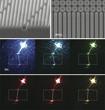
Nanoscale hyperbolic metasurface fashioned in silver film (top row) showed negative refraction at wavelengths shorter than 540 nm (middle row) and normal refraction at longer wavelengths (bottom row). [Image: Courtesy of Robert Devlin, Harvard University]
A team of U.S. scientists has developed a 2-D “hyperbolic metasurface” that can exhibit classic metamaterial properties, such as negative index of refraction, at the scale of integrated photonics—and with optical losses two orders of magnitude lower than in bulk metamaterials (Nature, doi: 10.1038/nature14477). In addition to low loss and propagation without diffraction, the new surface enabled wavelength-dependent control of the refraction and routing of visible light. The team believes that the work “open the door to realizing integrated optical metacircuits,” with applications in imaging, sensing, and quantum information.
The quirky optical properties of metamaterials and their promise of unusual applications have been known for decades. But bringing those properties to the chip scale has posed a challenge. Bulk metamaterials—difficult in any case to integrate into flat photonic chips—also exhibit high propagation losses, as optical energy is absorbed by the metallic components that typically constitute part of the metamaterial design.
One possible solution lies in so-called hyperbolic metasurfaces, strongly anisotropic, planar designs that allow the light’s electromagnetic energy to propagate along a metal-dielectric interface as surface plasmonic polariton (SPP) waves. Such 2-D metasurfaces, more easily integrated into flat optoelectronic circuits, should thus also show much lower losses than bulk metamaterials—with the same exotic characteristics, such as negative refractive index. But their properties have heretofore been mainly the stuff of theory, and haven’t been experimentally realized in the visible wavelength band.
To put the theory into practice, Alexander High and OSA student member Robert Devlin—members of a team supervised by OSA Fellow Mikhail Lukin and Hongkun Park of Harvard University (USA)—used sputter deposition of a single-crystalline silver film, followed by sophisticated electron-beam lithography and plasma etching that cut nanoscale ridges into the silver crystal. The result was a metasurface precisely tuned for creating surface plasmon energy waves at visible frequencies at the air-silver interface. As predicted by theory, propagation losses of energy supplied by a coupled excitation laser, and traveling along the metasurface as SPP waves, were 100 times less than those experienced in bulk metamaterials.
The team demonstrated that this low-loss material also showed a negative index of refraction—a hallmark of metamaterials. Perhaps more remarkably, the refractive-index behavior was wavelength-dependent, with refraction pivoting from normal at wavelengths longer than 540 nm to negative at shorter wavelengths. And in one of their experiments, the researchers unveiled what they describe as a “new optical phenomenon,” the dispersion-dependent plasmonic spin-Hall effect, under which light can be routed with left or right circular polarization depending on wavelength.
Lead co-author Devlin suggests that the combination of low-loss and 2-D geometry could “open up the possibility for chip-scale routing of light,” potentially even at the single-photon level. And, while the demonstration involved a silver-air grating, the team believes that the general approach is compatible with other materials and techniques common in the semiconductor industry.