
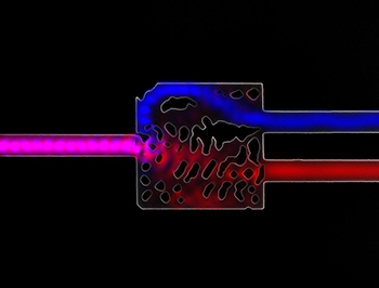
IR light enters the silicon-on-insulator demultiplexer from the left. Algorithm-determined cutouts split the two wavelengths into separate channels on the right. Credit: Alexander Piggott, Stanford University
Integrated photonic components will become key building blocks of future computers and communications devices. However, the experts who design computers aren't necessarily optical scientists—and designing tiny optical components usually requires brute-force optimization of parameters and deep experience with photonics.
To make optoelectronic components smaller and easier to design, researchers at Stanford University (USA) used their inverse design algorithm to build a silicon-on-insulator wavelength demultiplexer only 2.8 µm on a side (Nature Photon., doi:10.1038/nphoton.2015.69).
Typical optoelectronic multiplexers and demultiplexers contain components that are 10 to 20 µm in diameter, said Jelena Vučković, professor of electrical engineering at Stanford. Her graduate student, Alexander Piggott, was the lead author on the study. Additionally, designers of integrated photonic circuits have had to rely on “analytic theory and intuition” and then optimize the design using a limited number of degrees of freedom, the authors wrote.
In the current study, the Stanford team employed their inverse design algorithm (Opt. Express, doi:10.1364/OE.21.013351), which takes the desired specifications for an optoelectronic structure and searches through all possible topologies to find the perfect design. Today's design software for ordinary electronic devices works the same way—the user can plot complex circuits without worrying how each building block works.
The resulting demultiplexer structure doesn't resemble any kind of simple geometry—Vučković says it looks “like a block of Swiss cheese”—but it separates a mixed 1,300-nm and 1,550-nm light signal into two channels with less than -11 dB of crosstalk. The researchers inscribed the silicon demultiplexer on a silicon dioxide substrate using standard electron-beam lithography.
“A lot of functions in nature are done efficiently with structures that look very aperiodic,” Vučković says.
Structures as small as the demultiplexer in this study could be used as optical interconnects between cores on a next-generation computer processor, Vučković says. In the near future, her team will apply the process to more complex optoelectronic structures.