
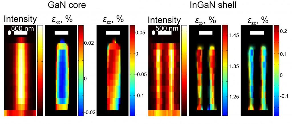
X-ray images of each nanowire show the distribution of the scattering intensity and the mechanical strain in the GaN core and the InGaN shell. The strain shows that the shell fits perfectly with the core. [Image: Tomaš Stankevič, Niels Bohr Institute, University of Copenhagen]
Nanowire LEDs—tiny semiconductor rods standing on end like trees in a miniature forest—could soon provide energy-efficient lighting for smartphone screens and other devices. To bring that technology to fruition, though, researchers need to optimize the core-shell configuration of the nanowires and to reduce lattice defects.
A Denmark-based team of scientists recently used a narrow, tightly focused X-ray beam to map the strain levels of individual nanowire LEDs grown on a sapphire substrate (ACS Nano, doi: 10.1021/acsnano.5b01291). The distribution of the mechanical strain within a nanowire can reveal crystal lattice discontinuities that reduce their efficiency, says Tomaš Stankevič, a doctoral candidate at the University of Copenhagen's Niels Bohr Institute and lead author of the study.
Green LEDs are less efficient than their red and blue cousins, especially at higher energies, Stankevič says. If scientists can design green LEDs that match other LEDs in emission and efficiency, they could build light sources with improved color rendering. (Today's “white” LEDs are blue LEDs behind a yellow phosphor, resulting in a cool-white tone.)
Scientists created the nanowire LEDs, which are roughly 400 nm in diameter and 4 μm tall, by selective-area metal-organic chemical vapor deposition. These LEDs give off light at 428 nm. The stalks contain layers of gallium nitride and indium gallium nitride built up around a gallium nitride core. The group scanned a “forest” of these nanowires with a tightly focused X-ray beam and studied the resulting fluorescence and diffraction images.
The new scanning technique allowed the researchers to visualize the mechanical strains in individual nanowires despite their location in an ensemble, according to Stankevič. The resulting images also showed that some of the nanowires are slightly twisted and tilted with respect to each other. “In general, they should be straight as soldiers, but they are tilted,” Stankevič says. “We still have to find out why they are tilting.”
The team performed the scans at the DESY synchrotron laboratory in Hamburg, Germany. Recent advances in X-ray optics allowed the team to focus the 24.3-keV beam down to a width of 100 nm, according to Stankevič. He and his colleagues plan to use Sweden's more advanced synchrotron, MAX IV, for future experiments with an X-ray beam focused to a width of only 10 nm, which could result in improved strain-mapping resolution.
Researchers from Technische Universität Dresden (Germany), Lund University (Sweden), Glo AB (Sweden) and Glo-USA Inc. (Sunnyvale, Calif.) also participated in the study.