
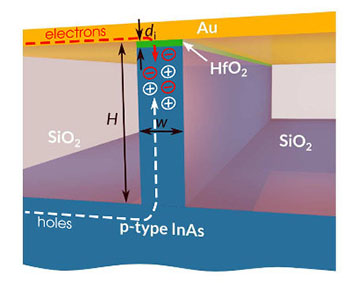
Inserting a thin layer of insulator between metal and semiconductor in an electrically pumped plasmonic waveguide blocks hole transport while allowing efficient electron transport, creating a population inversion in the semiconductor and providing optical gain that can compensate for surface-plasmon energy loss. [Image: Svintsov et al., Opt. Express, doi: 10.1364/OE.23.019358]
Optoelectronics researchers in Russia have proposed a new design for a fast plasmonic chip, with the potential to dramatically cut the large energy losses that have typically blocked practical use of such devices (Opt. Express, doi: 10.1364/OE.23.019358). While the initial results await experimental verification, the team leader, Dmitry Fedyanin of the Moscow Institute of Physics and Technology (MIPT), believes that they “clear the way for the development of a new generation of high-performance optoelectronic chips.”
Plasmonic components on integrated circuits—in which energy from light is concentrated into surface plasmon polaritons (SPPs), sub-wavelength electromagnetic oscillations that can propagate along a metal-dielectric interface—have significant promise for enabling large-scale integration in nanoscale optoelectronic chips and devices. That’s because SPPs offer the potential for breaking the diffraction limit imposed by the micrometer-scale wavelength of light in conventional waveguides, and allowing for the nanometer-scale integration common in electronic chips.
But there’s a catch: SPP propagation requires a metal interface, and that means that the electric field attenuates quickly through absorption in the metal—dropping off, according to Fedyanin, a billion times at distances of around a millimeter. And, while it’s possible to compensate for these losses by pumping additional energy into the system, the optical pumping schemes demonstrated thus far to do so have required a large, impractical energy input.
Fedyanin and his team looked at an alternative approach for overcoming surface plasmon energy loss: pumping energy into the system not optically, but electrically. Specifically, the scheme involves inserting a very thin layer of insulating material between the metal-semiconductor interface in the plasmonic waveguide. The insulating layer serves a dual purpose, allowing efficient injection of minority carriers (electrons, in this case) while blocking majority-carrier (hole) current.
The added insulating layer helps to suppress leakage current and ohmic losses in the metal layer. And, when a forward bias voltage is applied, it allows a sufficient concentration of electrons near the semiconductor-insulator-metal interface to create a population inversion in the semiconductor and provide optical gain for the plasmonic mode propagating in the waveguide—amplification that compensates for SPP propagation losses.
In numerical models of the geometry, using a hypothetical system with gold as the metal layer, hafnium dioxide as the insulator, and the p-type semiconductor indium arsenic, the team calculated that the system could fully compensate for SPP propagation losses “at a current density of only 2.6 kA/cm2.” Replacing gold with copper, which significantly increases the minority-carrier injection efficiency, dropped the required current density to 0.8 kA/cm2. “Such an exceptionally low value,” the study concludes, “demonstrates the potential of electrically pumped active plasmonic waveguides and plasmonic nanolasers for future high-density photonic integrated circuits.”