
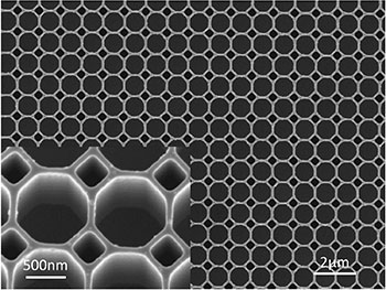
Scanning electron micrograph of the fabricated superlattice photonic crystal, etched 2.2 μm deep into a tantalum substrate. [Image: V. Rinnerbauer et al., Optica, doi: 10.1364/OPTICA.2.000743]
Most of us are familiar with the basic principles of solar cells, which convert incident light directly to electricity. But there’s another road to solar-driven electricity: so-called thermophotovoltaics (TPVs), in which sunlight or other radiation is captured as heat and re-emitted at a narrower wavelength band to drive the photovoltaic cell. Scientists from Austria and the United States recently unveiled a new design for a key component of such systems—one that the researchers believe could make TPVs considerably more practical for large-scale deployment (Optica, doi: 10.1364/OPTICA.2.000743).
In a TPV system, radiation from the sun, combustion, or another heat source, rather than directly illuminating a solar cell, falls on an intermediate surface—typically a photonic crystal—that absorbs incident radiation at a range of wavelengths, and then churns out photons, via thermal emission, at a narrower wavelength band suitable for driving photovoltaic electricity. In principle, such systems can have efficiency advantages over direct photovoltaic systems, which commonly use a much lower share of incident solar energy. TPVs can also be driven by power sources other than the sun, such as combustion, in winter months when sunlight is scarce.
The challenges: High temperatures, spectral selectivity
Despite those potential advantages, though, it’s been challenging to bring TPV systems to wide deployment. One reason for that lies in the highly specific demands on the photonic crystal that does the heavy lifting of thermal absorption and re-emission. For one thing, the material must be stable at extremely high temperatures, on the order of 1,500 K, over a long working lifetime.
Further, while they can use a larger share of incident radiation than in direct solar-cell systems, the crystals in TPV systems still must be spectrally selective—that is, they must absorb only the wavelengths that can efficiently be thermally re-emitted as photons in the appropriate, narrower wavelength band for their final photovoltaic destination. Otherwise, the system efficiency will suffer, with energy bleeding off as waste heat. While some promising 2-D photonic crystal designs have been devised, fabrication of them has been too expensive for production of large-area absorbers.
Building an ultraselective abosrber
To create a more practical absorber-emitter for TPV, a team of scientists from the Johannes Kepler University and the Technical University (Austria) and from the University of North Carolina and the Massachusetts Institute of Technology (USA) brought a combination of techniques to bear. The researchers first modeled a 2-D “superlattice” metallic photonic crystal of alternating octagonal and square cavities. The dimensions and geometry were numerically optimized for resilience at high temperatures, and for high spectral absorption between 300 and 1,900 nm—with steep cutoffs outside of that range. They then fabricated the geometry on polished tantalum substrates using ultraviolet nanoimprint lithography (UV-NIL), in which the complex, intricate geometry is patterned onto a transparent stamp, mechanically pressed into a “resist” surface, and then hardened by exposure to ultraviolet light through the transparent stamp.
The result, according to the team, was a superlattice surface that can potentially provide solar absorptivity of 96 percent and a thermal transfer efficiency of 82.8 percent at operating temperatures of 1,500 K. And, the scientists conclude, the UV-NIL fabrication technique is sufficiently general and cost-effective to open a path to “high-throughput, high-resolution fabrication of complex high-temperature photonic components.”