
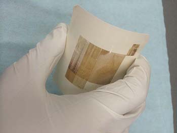
High-mobility polysilicon layer on paper. Credit: R. Ishihara, M. Trifunovic/TUDelft
Scientists have been racing to create electronic circuitry that would be as easy to print on a flexible substrate as it is to print a document on paper. Now an international team of researchers has figured out how to laser-print thin-film silicon transistors directly onto paper (Appl. Phys. Lett., doi:10.1063/1.4916998).
Over the past six years, various groups have experimented with organic and metal-oxide semiconductors, which exhibit less field-effect electron mobility than silicon. Others have tried using a type of silicon precursor that is liquid at room temperature to print circuits onto substrates, but that kind of “silicon ink” needed an intermediate step of amorphous-silicon formation, followed by annealing at 350 ºC, which would harm some inexpensive flexible materials.
In the new research, a team led by Ryoichi Ishihara of the Delft University of Technology (Netherlands) applied the silicon precursor, cyclopentasilane, to paper with a thin blade in an oxygen-free environment. The scientists then hit the “ink” with 28-ns pulses from a xenon-chlorine excimer laser operating at 308 nm. The ultraviolet blasts transform the cyclopentasilane into polycrystalline silicon.
Because of the short laser pulses, thermal energy has no time to diffuse into the substrate and damage it. The researchers created the thin-film transistors at a maximum temperature of only 150 ºC. By changing the energy density of the pulses, the team could change the type of solid silicon they were creating—polycrystalline, amorphous or microcrystalline. Raman spectroscopy confirmed the changes in the structure of the silicon.
The group used a special kind of coated paper, with an average roughness of less than 20 nm, to print the silicon circuitry, which turned brown as it solidified. Leaving the printed transistors exposed to room air for nine months did not alter their structure, as another round of Raman spectroscopy revealed. The transistors showed output properties comparable to other types of n- and p-type transistors, with field-effect mobility of up to 23.5 cm2/Vs.
Potential uses for the printed transistors include low-cost radio-frequency identification tags, wearable sensors and other flexible devices.
Researchers from the Japan Advanced Institute of Science and Technology also participated in the experiments.