
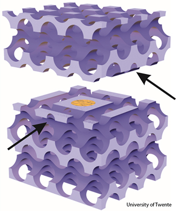
A prison for light in a diamond-like photonic crystal. The top-side of the crystal has been lifted to reveal the inner structure. The crystal has a diamond-like structure, made of two sets of mutually perpendicular pores that are drilled in silicon. To realize a resonant cavity, one pore in each set (black arrows) has a smaller diameter. At the intersection of these two pores, a point defect appears in the crystal. Light is confined in a tiny volume about this point (yellow region).
In nanophotonics, trapping light is as important as letting it flow. Building optical cavities into 3-D photonic crystals is challenging, however, because designers need to change the repeat structure deep down in a crystal's innards.
Scientists at the University of Twente, the Netherlands, have developed a model for a resonant nanocavity inside a 3-D inverse-woodpile photonic band gap crystal (Phys. Rev. B, doi: 10.1103/PhysRevB.90.115140). A point defect at the intersection of two perpendicular pores, with one pore of smaller radius than the other, localizes the electric-field energy and thus acts as a cavity.
The group, led by Léon Woldering and Willem Vos of Twente's MESA+ Institute for Nanotechnology, performed extensive computer simulations of a 5 ˟ 5 ˟ 5 supercell structure to find the optimal pore radius. The researchers showed that the electric-field energy is trapped within a mode volume of 0.8 cubic wavelengths—in other words, the light is strongly confined.
The Twente team now seeks to modify their CMOS-compatible manufacturing techniques to fabricate silicon photonic crystals with embedded optical cavities that will work at telecommunications wavelengths (1,270 and 1,550 nm). According to the researchers, the cavity design could work with photonic crystals made from other semiconductor compounds to capture light at shorter wavelengths. Ultimately, the photon confinement method could be used in designing efficient miniature lasers and LEDs, on-chip memory storage and sensors.