
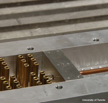
One end of the photonic crystal. The input cable is on the right, with the antenna in the center and to the left the array of metallic posts. The top plate of the photonic crystal was removed to take the picture.
On the way to their goal of building a compact free-electron laser, several researchers at the University of Twente (Netherlands) figured out how to map the intensity distribution of the radiation within a photonic crystal (Opt. Express 20, 22902).
The team was building a free-electron laser in which the electrons pass through photonic crystals, said Thomas Denis, a Ph.D. student at Twente’s MESA+ Institute of Nanotechnology. Because of the strict design requirements of the laser, the researchers wanted to measure what was going on inside the photonic crystals, so Denis and his colleagues designed a separate experiment to develop a measurement technique.
The scientists built a photonic crystal of vacuum and periodically ordered metal rods inside a cavity with mirrored ends and measured frequencies that could exist inside the crystal. Then they inserted a single metal bead, smaller than the wavelength of radiation used in the experiment, which could be positioned at various distances from the side of the crystal.
The scattering of light around the bead perturbed the electric field and changed the resonant frequency of the photonic crystal, and the team measured these frequency shifts as a function of the position of the scatterer. Thus they obtained a map of the dominant electric field component Ez inside the photonic crystal.
For ease of fabrication, Denis and his colleagues built this photonic crystal to work with microwaves at the millimeter scale. For the design of his free-electron laser, however, he would like to repeat the experiment in the terahertz regime. The researchers suggest that this technique could work at infrared and visible wavelengths by attaching a tiny scatterer to an atomic force microscope by means of a carbon nanotube.
“For us in this path of research, it was just a sidetrack that we explored for a specific application, but we realized that this small sidetrack investigation might be interesting for a broader public,” Denis says.