
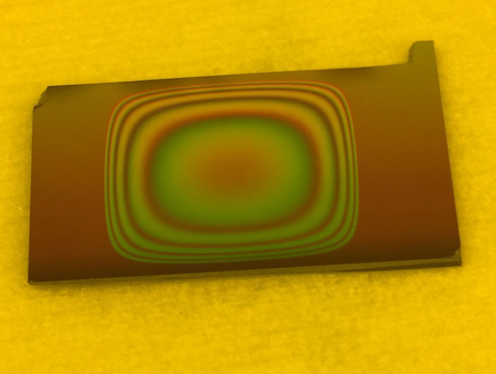
Beauty from a Fabrication Error
This beautiful pattern appeared randomly on the sample due to fabrication mistake. A thin-film, deposited on a silicon dioxide sample, and it had a rectangular shape. Once I put it inside the PECVD chamber to deposit silicon dioxide on top to protect it, instead, I accidentally ran the PECVD clean process, which uses very high RF power with gases that started to remove the thin film. It created this symmetric pattern on the sample surface.
—Amirmahdi Honardoost, CREOL, The College of Optics & Photonics, University of Central Florida, USA