
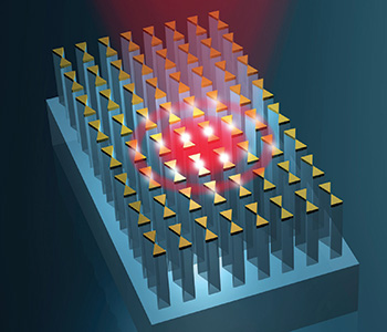
 Artistic representation of pillar-supported bowtie nanoantennas. [Phil Saunders/spacechannel.org]
For those of a certain generation, “antenna” conjures up early childhood memories of “rabbit ears”—telescopic, upward-pointing metal rods—perched on top of a television. Childhood observations allowed us to infer a few things about antenna functionality with no knowledge of antenna theory or electromagnetics. We observed that antennas were metal and typically long, and that the antenna’s relative orientation was crucial to signal reception. We might even have made an educated guess that antennas somehow converted the “television waves” of our favorite program, beamed through the air from the broadcasting station, into a signal that our television set could translate.
With the advances in personal electronics and communication devices over the last several decades, antennas have become ubiquitous. We generally are oblivious to their presence, however, because of their ubiquity and their increased miniaturization. Cellphone technology, for example, has moved from using carrier frequencies on the order of hundreds of MHz to a few GHz; this, in turn, has reduced the size of cellphone antennas from externally mounted projections to devices small enough to be concealed within the body of the cellphone itself. That’s because the characteristic dimensions of the antenna are proportional to the order of the radiation wavelength—and, thus, higher-frequency, shorter-wavelength devices will require smaller antennas.
By the same physical logic, an antenna for light—an electromagnetic wave oscillating at THz frequencies—would require nanoscale dimensions. And developments in nanotechnology in recent years have made the fabrication of optical antennas, or nanoantennas, quite viable. The ability of these devices to convert optical radiation to spatially concentrated energy at the nanoscale has found application in areas as diverse as data storage, spectroscopy, and sensing, as well as in nanoscale optical tweezers. And our group has recently shown that optical nanoantennas can even be modified to serve as photographic film for recording images or encoding sound in the near field—a finding that opens some fascinating potential new applications for the devices.
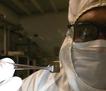 A pillar-supported bowtie nanoantenna chip. [PROBE Lab/University of Illinois]
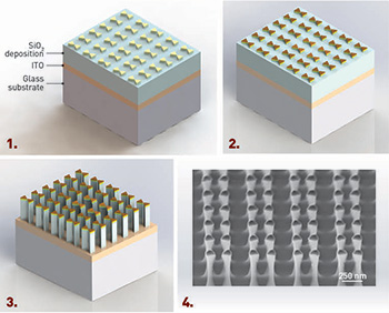 Steps in making pillar-supported bowtie nanoantennas (p-BNAs): 1. E-beam lithography and metal evaporation; 2. Deposit hard mask (Ni); 3. Reactive ion etching; 4. SEM image of p-BNAs.
From theory to fabrication
Optical nanoantennas do not operate in quite the same way as their radio and microwave counterparts—particularly because metals are appreciably lossy at optical frequencies. Instead, nanoantennas operate via localized surface plasmon resonance (LSPR), a collective oscillation of the free electrons in noble metals.
Associated with LSPRs is the confinement and enhancement of incident light in the near field. Known as the lightning-rod effect, this is particularly strong near sharply curved tips or within nanoscale gaps. The remarkable ability of nanoantennas to squeeze light into sub-diffraction volumes stems from the fact that the kinetic energy of the oscillating electrons greatly outweighs the magnetic energy in the near field. As such, LSPRs are governed by electromechanical energy, as opposed to the electromagnetic energy of freely propagating waves. This further explains the geometric tunability of LSPRs: the antenna shape alters the electron energy distribution.
Although nanoantennas formed from chemically synthesized, discrete plasmonic nanoparticles are of interest particularly for basic-science studies, nanoantenna structures fabricated in organized patterns or arrays are more intriguing for actual applications. The former, “bottom-up” approach to fabrication includes solution phase synthesis, which exploits the interactions of atoms or molecules to organize the nanostructures on a substrate. The “top-down” fabrication approach, by contrast, typically involves either electron beam lithography (EBL) or focused ion beam (FIB) lithography to provide precise control over the dimensions of the fabricated nanostructures. EBL tends to be more suited for mitigating potential substrate damage, whereas FIB lithography can be used to directly pattern devices from a metal film.
The nanoantennas used in our research are fabricated by EBL in a 2-D array geometry on glass substrates coated with a thin layer of indium tin oxide (ITO). A single nanoantenna comprises of a pair of gold equilateral triangles arranged tip to tip, with a nanoscale (dielectric) gap of roughly 20 to 30 nm, depending on the application. These so-called bowtie nanoantenna arrays (BNAs) have a geometric configuration quite favorable to LSPR tunability (for example, by changing the gap size) and offer more than a thousand-fold enhancement of the local field intensity in the gap region.
By placing BNAs on 500-nm tall silicon dioxide pillars (using reactive-ion etching of the substrate), a mechanical degree of freedom can be introduced: these pillar-supported bowtie nanoantennas (p-BNAs) can be actuated by the gradient force induced by a strong electromagnetic field, such as that from a standard scanning electron microscope. That, in turn, can result in a narrowing of the nanoscale gap region down to a size that is approximately 0.01 times the wavelength of visible light.
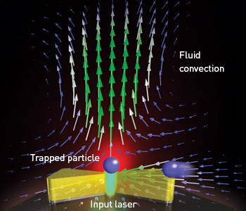 Nanotweezers in action: In plasmonic nanotweezers, electromagnetic forces from the laser are amplified in the antenna gap, forming an optical trap; as the antennas are heated by electron motion, convection currents draw particles into the trapping volume surrounding the illuminated spot.
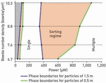 A trapping phase diagram shows the different particle sorting regimes enabled by different parameters, for different particle sizes. [Adapted from Roxworthy et al., Nano Lett. 12, 796 (2012)]
Plasmonic nanotweezers
The deep subwavelength confinement and strong field enhancement associated with LSPRs combine to generate large near-field intensity gradients. Thus substantial amplification of optical gradient forces can be realized with nanoantennas, an effect that forms the basis of state-of-the art plasmonic nanotweezers for optical manipulation.
Plasmonic nanotweezers use metallic dimers as nano-focusing elements to concentrate incident electric fields into an engineered gap. The result is a pronounced increase of the trapping efficiency: Q = Ftot cm/P, where Ftot is the total trapping force, cm is the speed of light in the trapping medium, and P is the incident optical power. A value of Q = 1 implies that all of the incident optical momentum is converted to trapping force on an object. The augmentation of Q enables low-input-power particle manipulation with remarkable trap stiffness and total force.
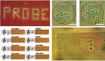
To that end, nanotweezers have featured a wide variety of geometries, including disks, rods, blocks and bowties. Concurrent with the resonant field enhancement, nanotweezers can also produce significant heating of the surrounding fluid medium containing the target particles. While this effect has generally been regarded as deleterious to trapping performance, our group has shown that by carefully tuning the resonance conditions—such as input wavelength and optical power—a rich set of trapping dynamics can be realized for micron-sized particles.
In these systems, the delicate balance between optical and thermally induced forces, generated by off-resonance illumination of dense arrays of bowtie nanonantennas, can produce different trapping states, or phases. Below a given power threshold, efficient single-particle trapping with Q > 1 is possible, which provides direct evidence that non-optical forces can contribute favorably to trapping performance. Above this empirically determined threshold, convective forces destabilize the single-particle trap, but multiple particles can be trapped simultaneously. By exploiting the particle-size dependence of these fluid forces, nanotweezers can be used for passive particle sorting.
Plasmonic nanotweezers are particularly attractive in their potential application to manipulating live biological specimens. Interrogation of biological systems using conventional optical tweezers has already borne remarkable fruit, providing key insights into the operation of motor proteins and mechanical properties of nucleic acids. But application of the full power of optical tweezers to any biological specimen runs the risk of specimen damage due to intense optical radiation. Plasmonic antennas, by contrast, use much lower input power densities, and are also amenable to incorporation into optofluidic systems.
Moreover, conventional optical tweezers, being subject to the diffraction limit, have trapping volumes limited to hundreds of nm3—too large for confining nanoscale objects that are significantly perturbed by Brownian fluctuations. The extreme light confinement offered by plasmonic nanoantennas can reduce trapping volumes down to tens of nm3, and plasmonic nanotweezers have been employed for manipulation of individual proteins and dielectric objects with dimensions as small as 12 nm.
An emerging area of interest for plasmonic nanotweezers is the use of a femtosecond pulsed excitation source. Pulsed light offers a potentially useful route for improving the nanotweezer trap stiffness, and could also open up new regimes of particle dynamics, in which objects can be selectively fused to plasmonic structures using mere microwatts of average power. This effect could be employed to modify the optical response of selected antennas, offering a route for novel sensing modalities or studies in nonlinear optics.
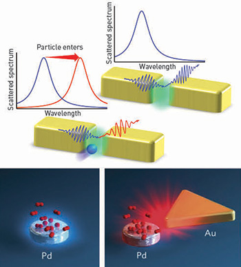 Plasmonic sensors: (Top) The increase in local refractive index in the plasmonic “hot spot” leads to a pronounced redshift in scattered light from the nanoantenna when the particle to be sensed enters the hot-spot region. (Bottom) Schematic view of hydrogen gas sensing near a palladium nanoparticle, where a gold nanoantenna dramatically increases measurement sensitivity. [N. Liu et al., Nat. Mater. 10, 631 (2011); © Macmillan Publishers Ltd. Reprinted by permission.]
Plasmonic sensors
The lossy nature of noble metals at optical frequencies can be exploited for sensing applications. Specifically, such loss gives these metals a complex frequency-dependent dielectric function (or refractive index) ε(ω). In the case of a spherical plasmonic nanoparticle, for example, this means that its polarizability α(ω) is proportional to [(ε – εm)/( ε + 2εm)], where εm is the complex dielectric function of the surrounding medium.
Hence, the LSPR condition for this particle occurs when the real part of ε(ω) = –2εm. Different nanoparticle geometries will result in their own resonance condition. This strong divergence of the applied electric field, along with the field’s subwavelength confinement, leads to remarkable sensitivity to changes in the refractive index of the surrounding medium, and thereby makes nanoantennas ideal candidates for sensor applications.
Plasmonic nanoantennas have shown potential for sensitive detection of flammable gases such as hydrogen. The absorption of hydrogen by a single palladium (Pd) nanoparticle was detected as a shift in the LSPR of a gold nanoantenna placed in close proximity. A basic interpretation of the phenomenon is that hydrogen absorption by the Pd nanoparticle results in a change in the complex dielectric function of the Pd nanoparticle; consequently, the nearby plasmonic nanoantenna exhibits a corresponding plasmon resonance shift that can be optically detected.
Pillar-supported or freestanding nanoantennas constitute even better candidates for sensing than their substrate-bound counterparts, due to their higher sensitivity to the local dielectric environment. Gold-coated mushroom arrays on photoresist pillars have been fabricated and used as biosensors to detect the proteins cytochrome c and alpha-fetoprotein. And freestanding nanoantennas have been shown to be especially advantageous for surface enhanced Raman spectroscopy (SERS) of adsorbed molecules on metal surfaces, as they expose a larger fraction of the enhanced-field region, or “hot spot,” to the environment containing the analytes of interest, and as raising the nanoantennas above the substrate increases the refractive-index sensitivity. In one case, 3-D star-shaped metallic Au nanostructures fabricated on silicon pillars were shown to be sensitive enough to detect single molecules by SERS, and to detect Raman signals from adenine molecules at concentrations as low as ~1 pM.
Enhancing data storage
Advances in magnetic recording have pushed data storage density to several hundred terabytes per m2, about half of the theoretical limit. Even so, to meet the burgeoning demand for more storage capacity, magnetic grain sizes must continue to decrease. But reduction in grain size for materials such as Fe, Co, and Ni results in thermal instability as the grains become superparamagnetic—and alternative materials that can achieve the desired nanometer grain sizes exhibit magnetic anisotropy beyond what can be handled by the magnetic switching fields of conventional recording heads.
Plasmonic nanoantennas offer an approach to mitigating this latter issue. Specifically, a uniquely designed nanoantenna, optically excited at its LSPR in either the visible or near-infrared, can exploit the lightning-rod effect to funnel electromagnetic energy to a nanoscale region. This, in turn, can locally heat a desired subwavelength spot of the magnetic material to above its Curie temperature (roughly 350 °C for FePt) and, in turn, radically reduce the coercivity of the heated region, so that the available switching field of the standard head is sufficient to record data.
While this approach to magnetic recording faces a number of challenges (among them, improving the coupling between the optical field and the nanoantenna, and increasing both the field confinement and local field intensity enhancement), it offers strong potential for extending the limits of next-generation magnetic storage devices.
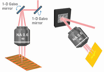 Plasmonic photography: Using either galvanometer-based steering mirrors (left) or a spatial light modulator (right), a standard microscope is used to encode information. [B.J. Roxworthy et al., Nano Lett. 14, 4687 (2014), © American Chemical Society]
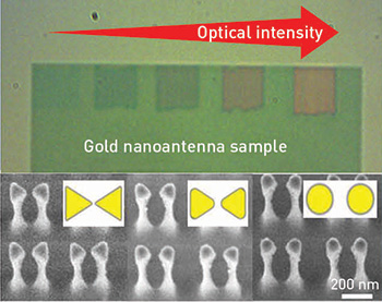 Information is encoded on an array of gold nanoantennas (bottom) through subtle surface melting of the metal and a consequent change in the plasmonic response. [H. Chen et al., Sci. Rep. 5, 9125 (2015)]
 Possible applications include stored images (top, left), encoded audio (bottom, left), or prewritten channels for optically guiding particles (right). [H. Chen et al., SPIE NanoScience + Engineering, 91641M-7 (2014) © SPIE]
Plasmonic photography
Our group has recently shown that the p-BNA flavor of nanoantennas can be adapted to record the optical intensity in the near field. Owing to the subtle surface melting that occurs in the metal upon resonant excitation, morphological changes occur in the form of increased radius of curvature of each bowtie tip, increased gap spacing, and reduced in-plane height of each nano-triangle. (Interestingly, even though the bulk melting temperature of gold, the metal used for p-BNAs, is greater than 1,000 °C, surface melting causes this temperature to be significantly reduced at the nanoscale.)
The end result of these shape changes is a shift of the LSPR of up to 100 nm. Therefore, depending on input power, wavelength and polarization, the near-field intensity exposure history can be recorded by the p-BNAs in a manner that resembles classic photographic film. Compared with traditional film, the “development” in plasmonic photography happens in real time, thereby enabling instant feedback to nanoscale changes. Moreover, an optical microscope rather than a conventional point-and-shoot camera is used to transduce the optical information from a subject onto the plasmonic film—an effect that occurs at subwavelength distances.
To use such a nanocamera, one can take advantage of increasingly common auxiliary microscope components such as beam-steering galvo mirrors or a spatial light modulator to record a variety of patterns on the film—in principle, down to the level of a single pixel or bowtie (roughly 200 × 200 nm). Using this approach, our group was able to record the world’s first movie encoded on nanoantennas. And—in a manner reminiscent of the early history of talking pictures, when audio information was optically encoded and stored on film for later playback—we have also shown that audio recording using p-BNAs is possible. Once again, a microscope is the platform used for recording; the desired audio signal modulates a pair of galvo mirrors such that the audio signal can be stored on the p-BNA film either as a time-varying waveform or in the frequency domain as the corresponding amplitude and phase spectra.
Aside from the obvious “cool factor,” the emergence of plasmonic photography using p-BNAs has worthwhile scientific and engineering applications. The technology could serve as a useful component in developing plasmonic-based on-chip signal processing, where unwanted frequency components can simply be ablated away.
Another application comes from the realization that the nanoantennas do not have to be ablated to effect a significant spectral shift in their LSPR response—indeed, visible color changes in the reflectivity of white light from a p-BNA chip can be observed for an input power as low as 100 µW (around 50 times less power than from a standard laser pointer), over a focused spot diameter just less than 700 nm. Thus, for nanotweezer applications, the local gradient force can be biased by spatially exposing selected regions to a particular dosage of light intensity. This effect can be used to fabricate “optofluidic channels without walls” that could prove very attractive for lab-on-a-chip applications.
Nanoantennas in the technology toolbox
Which application emerges as the “killer app” that takes plasmonic nanoantennas to the technological mainstream will depend on a number of next steps. Applications such as plasmonic circuits and direct light harvesting appear to be hampered by the fact that metals such as gold and silver are lossy and, in view of their expense, are generally not attractive for the silicon manufacturing infrastructure of the traditional semiconductor industry. This has led to emerging efforts to fabricate nonmetallic nanoantennas using alternative materials such as titanium nitride and silicon.
But, as some of the nascent research discussed above has highlighted, losses in one application domain may be viewed as a resource in another domain. That suggests that a potpourri of nanoantennas for concentrating light, with different characteristics to choose from, could drive a range of applications as their properties continue to evolve. Optical nanoantennas, like their long-wavelength counterparts, may eventually become just another—very useful—component in the toolbox.
Kimani C. Toussaint Jr., Hao Chen, Abdul M. Bhuiya and Qing Ding are with the PROBE Lab at the University of Illinois at Urbana-Champaign, Urbana, Ill., USA. Brian J. Roxworthy is a National Research Council Postdoctoral Researcher in the Nanofabrication Research Group at the National Institute of Standards and Technology, Gaithersburg, Md., USA.
References and Resources
-
P. Bharadwaj et al. Adv. Opt. Photon. 1, 438 (2009).
-
D. O’Connor and A.V. Zayats. Nat. Nanotech. 5, 482 (2010).
-
M.L. Juan et al. Nat. Photon. 5, 349 (2011).
-
N. Liu et al. Nat. Mater. 10, 631 (2011).
-
G.V. Naik et al. Opt. Mater. Express 1, 1090 (2011).
-
B.J. Roxworthy et al. Nano Lett. 12, 796 (2012).
-
B.J. Roxworthy and K.C. Toussaint. Sci. Rep. 2, 660 (2012).
-
M. Chirumamilla et al. Adv. Materials 26, 2353 (2014).
-
B.J. Roxworthy et al. Nat. Commun. 5, 4427 (2014).
-
H. Chen et al. Sci. Rep. 5, 9125 (2015).