
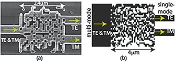
 (a) Scanning electron micrograph of the PBS (see video 1). (b) Design of a mode-converting PBS (see video 2). Light polarized in either state enters from the left waveguide and is separated into the orthogonal polarization states in the right waveguides.
The mainstay of all high-bandwidth information transfer is optical communications, whether it is between computer cores within a data center or via networked computers across the world. The vast majority of these signals are processed using expensive, power-hungry discrete devices. Integrating these devices can reduce power consumption and costs, and enhance reliability.
However, optical-information processing on chip is stymied because the wavelength of light limits the smallest device size. For example, an integrated polarization beam-splitter (PBS) can be as large as 100 μm2. Recently, we demonstrated a general approach to design that we call “digital metamaterials,” which use nanophotonic resonances both to drastically shrink the size of photonic devices and to enhance their functionality.1 Specifically, we demonstrated what we believe is the smallest PBS so far, with an area of only 5.76 μm2. Our device utilizes only non-absorbing materials, and their fabrication is compatible with standard silicon processes, thereby allowing manufacturing at large volume and low cost.
Non-intuitive optical properties have been demonstrated in metamaterials— for example, materials whose refractive index can be tailored in a spatially resolved manner. Digital metamaterials represent a further refinement in which we discretize the spatial variation, which enables fabrication-friendly and robust designs. Specifically, the device comprises discrete pixels whose geometric distribution is determined by an optimization algorithm.
Examples of integrated PBS devices include the smallest integrated PBS, only 2.4 μm in width, and a larger 4.0-μm-wide PBS that performs polarization splitting and mode conversion (see figure). This is an example of a multifunctional device enabled by digital metamaterials. Using this technique, we have also demonstrated free-space polarizers, free-space diodes, integrated diodes, and integrated free-space-to- waveguide couplers.2-5
Our application of topology optimization to the task of enhancing photonic functionality while decreasing the footprint of integrated photonic devices is an exciting opportunity for scaling integrated photonics. Indeed, we believe the computational techniques we have used to drastically shrink the size of photonic devices can be applied to create libraries of useful and versatile devices. Such design techniques can be extended to active photonic devices as well as to quantum optics in the future.
Researchers
Bing Shen, Randy C. Polson, Peng Wang and Rajesh Menon, University of Utah, Salt Lake City, Utah, USA
References
1. B. Shen et al. Nat. Photon. 9, 378 (2015).
2. B. Shen et al. Optica 1, 356 (2014).
3. B. Shen et al. Opt. Express 23, 20961 (2015).
4. B. Shen et al. Opt. Express 23, 0847 (2015).
5. B. Shen et al. Opt. Express 22, 27175 (2014).