
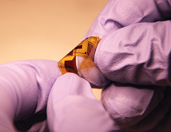
 This flexible photonic chip boasts excellent optical performance and extreme mechanical flexibility enabling repeated bending down to sub-millimeter radius without measurable performance degradation, both of which represent major improvements over other state-of-the-art devices.
In recent years, the increasing penetration of flexible devices into the consumer products market has led to a surge of interest in flexible photonics, i.e., integrated optical systems fabricated on flexible polymer substrates that can be mechanically deformed without compromising their optical performance. In addition to being an essential component in consumer electronics, flexible photonics also has enormous application potential for board-to-board optical interconnects, epidermal sensors, wearable photonics and flexible displays.
To date, most flexible photonic devices are made entirely from polymers. Unfortunately, polymer-based systems generally have small refractive index differences between their cores and claddings, resulting in weak light confinement, a large device footprint and excessive loss during bending. High-index-contrast semiconductor photonic devices can be alternatively fabricated using pattern transfer to overcome these limitations. However, the transfer process is complicated and has limited integration capacity. Further, the resulting devices only exhibit moderate flexibility with a bending radius typically no less than 5 mm.
This year, my colleagues and I created an integrated flexible chalcogenide glass photonic device.1 The device’s performance enhancement capitalizes on two innovations. First is the adoption of high-index chalcogenide glasses, namely the amorphous compounds of S, Se or Te as the backbone optical materials. Unlike oxide glasses, chalcogenides can be deposited at room temperature without compromising their low loss properties, thus facilitating monolithic photonic integration on plastic substrates. Second, a novel multi-neutral-axis micro-mechanical design is implemented to render the structure highly flexible. In the design, a soft silicone adhesive layer is sandwiched inside the flexible substrate, which serves to significantly relieve the strain in the composite structure. This design allows the photonic layer to be placed close to the surface, enabling access to the optical field for applications such as sensing.
Our monolithic integration route offers excellent device performance with high yield: our best optical resonator device exhibited an intrinsic Q-factor as high as 460,000, which we believe is the highest value reported in photonic devices on plastic substrates. Even after the membrane was bent many thousands of times at 0.8 mm bending radius, the devices maintain structural integrity and only a small increase (0.5 dB cm–1) in optical losses. These results open up emerging application avenues of flexible photonic devices where they can benefit from superior optical and mechanical performance.
We further exploited the monolithic integration approach to fabricate 3-D multilayer flexible photonic devices, including vertical interlayer adiabatic couplers, vertically coupled add-drop filters and 3-D woodpile photonic crystals. Compared to conventional 3-D stacking methods, our approach offers a simpler and more robust alternative for novel 3-D photonic structure processing.
Researchers
Juejun Hu, University of Delaware, USA
References
1. L. Li et al. Nat. Photon. 8, 643 (2014).