
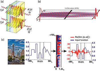
(a) Proposed concept. (b) Metasurface designed to perform first spatial differentiation, sandwiched between two graded-index slabs. (c) Layered metamaterial designed to perform second spatial differentiation on input profile, used to perform edge detection. [A. Silva et al. Science 343, 160 (2014). Austin city skyline photo courtesy of Tod Grubbs, Bee Creek Photography; reproduced with permission.]
Fast processing of large amounts of data has become increasingly important in a technologically demanding world.1 Nanoscale optics may bring new solutions into this arena. In recent work, we have presented one such application: a new paradigm for performing mathematical operations, using wave evolution in specially designed metamaterials.2
In our vision for wave-based “metamaterial analog computation,” an input wave with a given spatial profile propagates through an artificial material block designed to execute a specific mathematical operation, such as differentiation, and emerges at the output with its profile changed into the result of the desired operation. We have proposed two paths for this “photonic calculus”: specially designed subwavelength metasurfaces that operate in the spatial Fourier domain, combined with graded-index (GRIN) slabs or fibers; and layered metamaterials that engineer the desired operator’s Green's function directly in the space domain.
One simulated result using the first approach involves a metamaterial block designed to perform first spatial differentiation. In the simulation, we have applied the concept of meta-transmit-array (MTA)3 to design a metasurface that would use Si- and Al-doped ZnO—which exhibit positive and negative real parts of permittivity, respectively, at a 3 µm operating wavelength. This MTA is sandwiched between two GRIN slabs. In our simulations, the input field clearly evolves as it propagates through the system, exiting with a profile that resembles the input’s first derivative.
Our second approach is based on a stack of different layers performing second spatial differentiation on the input profile. The input wave—a skyline profile—propagates through a ten-layer block (with a total thickness of 1.2 wavelengths), performing second spatial differentiation on the profile. The output waveform sharply delineates the skyline edges, indicating that such a block can perform analog edge detection on the entire input image as light propagates through it. We have also designed structures that perform spatial integration and convolution.2
We have thus shown, theoretically and numerically, that light-matter interaction can be tailored to “do math with light.” Work is now under way to validate this concept experimentally. Such wave-based photonic calculus may open new avenues for handling and processing large data sets with unprecedented speed.
Researchers
A. Silva and Nader Engheta, University of Pennsylvania, Philadelphia, Penn., USA
F. Monticone and A. Alù, University of Texas at Austin, Texas, USA
G. Castaldi and V. Galdi, University of Sannio, Benevento, Italy
References
1. B. Jalali and M.H. Asghari. Opt. Photon. News 25, 24 (February 2014).
2. A. Silva et al. Science 343, 160 (2014).
3. F. Monticone et al. Phys. Rev. Lett. 110, 203903 (2013).