
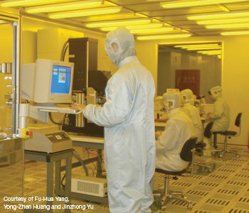
 Cleanroom of the Engineering Center for Semiconductor Integrated Technology, Institute of Semiconductors, Chinese Academy of Sciences, Beijing.
Integrated photonics can be defined as the science and technology of harnessing photons as they propagate and interact with micro- or nano-scale structures that are fabricated on a chip. The field is attracting significant R&D interest globally and making an impact on many high technological areas, including green information and communications technology, high-performance computing systems and on-chip biosensing.
Still, there are many stones that remain unturned. We have yet to make photonic-integrated circuits (PICs) similar to today’s standard integrated circuits (ICs)—with multiple functionalities, high performance and potentially low cost. This journey is expected to be very rewarding. China, which has been supporting discrete optoelectronic components research over the past three decades, has raised its R&D for integrated photonics over the past few years and has committed huge investments to it. As a result, many exciting results and proposals in this field are now emerging in China. This article aims to provide a glimpse into the rapidly evolving area of integrated photonics research in China.
The perspective given here is based on contributions from many leading research groups in China working on various aspects of integrated photonics research. Given the wide scope of activity, an exhaustive review of past and recent achievements and ongoing activities would be practically impossible. Thus, we will only look into national research programs in integrated photonics and highlight relevant research directions that have been recently funded. We will also showcase a few representative groups and their recent breakthroughs.
Integrated photonics research in China is a relatively young field compared to lasers and fiber optics, but it is on the rise. There is an increasing number of Chinese research groups delving into this area, and the amount of funding and number of published articles have grown as well. According to data from the Web of Science, the total number of publications (conference and journal articles) in integrated optics/photonics from China exceeded 2,000 over the past five years (2006-2010). This accounts for approximately 9 to 10 percent of the total number of publications in optics and photonics from China over the same period. China’s number of publications on integrated optics/photonics is consistently the highest in Asia and is second only to the United States.
National research programs
Two national research programs in China, called the 973 Program and the 863 Program, are funded and administered by the Ministry of Science and Technology. These programs are financing the integrated photonics R&D in China. The 973 Program, or Major State Basic Research Development Program, is China’s national program devoted to basic research. It is aimed at bringing together China’s scientific talents to conduct innovative research on major scientific issues related to sustainable development, such as information science and technology, energy, the environment, bioscience, etc. The 863 Program, or State High-Tech Development Plan, is aimed at stimulating technological R&D in areas of strategic importance to China’s economic and social development. Both programs typically span 4-5 years and involve team-based research with multiple principal investigators from many institutions in China, with a funding level per project on the order of tens of millions of renminbi.
National 973 basic research projects
 Silicon photonic devices recently developed at SJTU. These devices were fabricated at the open fabrication facility at Suzhou (a branch of the Chinese Academy of Sciences).
One of us (Jianping Chen) of Shanghai Jiao-Tong University (SJTU) is leading a recently funded 973 project (2011-2015), titled, “Key issues on photonic integrated chips for high-speed and low-power signal processing.” The participating institutions include Tsinghua University, the Huazhong University of Science and Technology (HUST), the University of Electronic Science and Technology of China (UESTC), the Beijing University of Post and Telecommunications (BUPT), the Institute of Semiconductors and the Institute of Microelectronics of the Chinese Academy of Sciences (CAS).
Through the project, the researchers seek to address the fundamental issues involved in peta-bits-per-second communication node processing in backbone networks—a capability that is expected to be implemented in China around 2020. The team proposes five optoelectronic chips on various semiconductor platforms (silicon, indium phosphide) and hybrid material platforms based on their functions in optical networking signal processing—namely (1) integrated chips for optical switching and buffering, (2) integrated chips for optical clock recovery, (3) 2R/3R regeneration ICs, (4) multi-channel all-optical format conversion chips and (5) optical tunable wavelength conversion chips.
Deren Yang of Zhejiang University leads another 973 project (2007-2011) titled, “Fundamentals of silicon-based light emission and optical interconnects.” Participating institutions include Peking University, Nanjing University and the Institute of Semiconductors of the CAS. The team has proposed and demonstrated various approaches for obtaining light emission from silicon-based materials, including silicon/germanium nanocrystals, rare-earth doping and hybrid technologies.
The team has also developed several advanced silicon nanostructures, including devices based on silicon-rich silicon nitride (SiN), nano-silicon multi-quantum-well (MQW) thin films, doped monodispersed nanocrystal silicon and rare-earth-doped silicon-rich silicon nitride/oxide. In addition, the researchers demonstrated tunable photoluminescence in the visible range based on silicon-rich SiNx films, and they have shown electroluminescence devices based on such SiNx films. Finally, they have developed two novel laser structures for silicon photonics, namely a selective-area metal bonding InGaAsP-Si laser (created by Guogang Qin’s group of Peking University) and an electrically pumped random zinc oxide laser grown on silicon in a metal-insulator-semiconductor structure (developed by Yang’s group).
Specifically, for the InGaAsP-Si laser, the InGaAsP MQW distributed feedback (DFB) structure was integrated into a silicon waveguide with the optical coupling and the metal bonding transversely separated. The laser operated with a threshold current density of 1.7 kA/cm2 and a slope efficiency of 0.05 W/A under pulsed-wave operation. The researchers realized room-temperature continuous lasing with a maximum output power of 0.45 mW.
Qihuang Gong of Peking University led a 973 project (2007-2011) titled, “Mesoscopic optics and novel micro/nano photonic devices.” In recent work, Xiao et al. studied a metal-coated microtoroid resonator system in detail. They found that this hybrid system supports a high-Q exterior plasmonic whispering-gallery mode (WGM), showing a high field locality that is concentrated in the exterior metal-dielectric interface.
These exterior modes are long-lived, and they enable interaction with external media such as microfluidics; thus, they hold great potential for various applications, including highly sensitive biosensors. Another major fundamental research direction that is being charted by Gong’s group is in the area of photonic crystal all-optical switching. Gong’s group demonstrated ultrafast (picoseconds) and low-threshold-power (100 kW/cm2 order) all-optical switching (80 percent efficiency) in two-dimensional composite photonic crystals.
National 863 high-tech projects
One of the recently funded 863 projects on “Photonics and monolithic integration research (Pamir)” (launched in 2010) is titled, “Photonic integration technology and its system applications.” Led by Ninghua Zhu of the Institute of Semiconductors, CAS, the project involves the following ten institutions: the Institute of Semiconductors, CAS; BUPT; Zhejiang University; Peking University; Nanjing University; the Wuhan Research Institute of Posts and Telecommunications; Southeast University; UESTC; Fudan University and Huawei Technologies Co., Ltd.
The main topics it will address are:
-
Ultra-small and ultra-high-capacity Si-based PIC
design and fabrication, -
Si-based monolithic photonic integrated 100 Gb/s
coherent receivers, -
InP monolithic integrated 10 x 10 Gb/s transmitters
for long-distance transmission, -
InP monolithic integrated 16 x 2.5 Gb/s transmitters
for wavelength-division multiplexing passive optical
networks applications, -
InP monolithic integrated 8 x 6 GHz transmitters for radio-over-fiber applications, and
-
System demonstration and applications.
Major projects from the National Natural Science Foundation of China
The National Natural Science Foundation of China recently funded a major project (launched in 2010), titled “Basic research on high-speed semiconductor integrated optoelectronic devices.” Also led by Ninghua Zhu of the Institute of Semiconductors, CAS, the project involves the following five institutions: the Institute of Semiconductors, CAS; Nanjing University; UESTC; Tsinghua University and SJTU. The main topics are:
-
10-channel InP transmitter PICs capable of a 100 Gb/s rate.
-
100 Gb/s all-optical wavelength conversion with a semi-conductor optical amplifier integrated with a distributed Bragg reflector laser.
Research highlights
Various key state laboratories, university labs and research institutions in China have demonstrated many “firsts” in China and the world for research relevant to integrated photonics. Here, we showcase a number of representative groups from Tsinghua University, CAS, Peking University, and Zhejiang University on work related to advanced laser structures, monolithic photonic integration technologies, photodetectors, silicon photonic devices and microsystems.
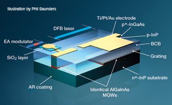
Over the past decade, Yi Luo’s group at Tsinghua University has been addressing significant issues in the design and fabrication of electroabsorption modulated lasers (EMLs), a key component for high-speed fiber communication systems. EMLs monolithically integrate a DFB laser with an electroabsorption modulator (EAM), and they constitute one of the most successful monolithic PICs to date. One key challenge facing researchers is figuring out how to realize wavelength compatibility, namely by ensuring that the DFB laser wavelength falls on the longer wavelength side of the excitonic peak of the EAM.
 Metal-coated silica toroidal microcavities. Schematic of a metal-coated silica toroidal microcavity supported by a silicon pillar. (Inset) False-color representation of the electric field for an exterior plasmonic WGM. Adapted from Yun-Feng Xiao et al., Phys. Rev. Lett. 105, 153902 (2010).
Luo’s group solved this problem by adopting the identical epitaxial layer (IEL) structure, in which the DFB laser and the EAM share the MQW layer. The IEL integration scheme greatly simplifies device fabrication, since no additional regrowth step is involved. Luo’s group was among the first in the world to propose and independently realize the IEL structure. By adopting the IEL integration technique and suppressing package-induced parasitic crosstalk between the laser and the modulator as well as optical and electrical crosstalk, Luo and his colleagues were the first in China to fabricate 2.5Gb/s, 10Gb/s and 40Gb/s EML transmitter modules in 1998, 2003 and 2007, respectively. Recently, Luo’s group demonstrated an EML module exhibiting an over 10-dB dynamic extinction ratio upon 43 Gb/s non-return-to-zero (NRZ) bit sequence modulation.
The research group of Wei Wang (an academician of CAS) in the Institute of Semiconductors, CAS, has been conducting research on InP-based semiconductor lasers and monolithic photonic integration technologies for the past two decades. One example of integrated photonic devices developed through Wang’s group is a tunable radio frequency source based on a three-section amplified feedback laser (AFL) design. The photonic integration is realized by using the quantum well intermixing technique, and the researchers demonstrated 32-51 GHz of continuous tuning. The group also established 40 Gbit/s all-optical clock recovery using this device. The AFL-extracted stable optical clock exhibited a timing jitter of 123.8 fs from a 40 Gbit/s return-zero pseudo-random bit stream (RZ-PRBS) pulse train.
Another example of developments made by Wang’s group is a sample-grating-based broadly tunable DFB laser array for high capacity transmission (a national 863 project). One prototype design is an array of eight sample grating tunable DFB lasers integrated with one combined output waveguide. Moreover, the researchers have designed and fabricated, in n-InP based materials, an optical logic gate based on evanescently coupled uni-traveling carrier photodetectors (EC-UTC-PD) integrated with an intra-step quantum well EAM. The EC-UTC-PD/EAM optical logic gate operated with an 8.4-dB extinction ratio and performed NRZ optical logic—while operating at 5 Gb/s.
In collaboration with Wang’s group, Zhu’s group of the Institute of Semiconductors, CAS, has demonstrated a monolithically integrated tunable microwave source using an EAM integrated with a DFB laser subject to optical injection. This source is particularly attractive due to its small size and wide frequency tuning range without using any cavity.
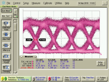 AlGaInAs laser chips. (Top) Identical epitaxial layer structure AlGaInAs multiple-quantum-well electroabsorption modulated laser chip. (Bottom) Measured 43 Gb/s eye diagram at voltage swing of 2 V. (Top) Adapted from C. Sun et al. in Proceedings of the 22nd IEEE International Semiconductor Laser Conference, Kyoto, Japan, 2010. (Bottom) Courtesy of Yi Luo and Changzheng Sun
One of us (Yong-Zhen Huang) heads another major research direction at the Institute of Semiconductors, CAS; it concerns the unidirectional emission of III-V semiconductor microcavity lasers for PICs. Unidirectional-emission semiconductor microcavity lasers fabricated by planar technique processes are potential light sources for PICs and on-chip optical interconnections. Huang’s group recently showed that integrating a bus-waveguide to an optical microcavity is a potentially simple way to realize unidirectional-emission microlasers.
The group has analyzed the mode characteristics of microresonators in various shapes and fabricated unidirectional emission microlasers on standard edge-emitting 1,550-nm laser wafers using an integrated bus-waveguide. They realized room-temperature continuous-wave injection lasing with device sizes down to 10 µm. The lowest threshold current demonstrated is 4 mA for an AlGaInAs/InP microcylinder laser with the radius of 10 µm. Furthermore, the group found that single-transverse-mode lasing is readily realized in hexagonal microlasers. Single-mode lasing with an SMSR of 33 dB was realized as well.
The group led by Qiming Wang at CAS has long been working on germanium-on-silicon (Ge-on-Si) materials for silicon-compatible near-infrared photodetectors. Ge-on-Si exhibits high absorption coefficients at the telecommunication wavelengths 1,310 nm and 1,550 nm, and it is compatible with silicon technology. The researchers grew Ge layers on Si and silicon-on-insulator (SOI) substrates using ultrahigh vacuum chemical vapor deposition based on lower-temperature buffer technology. The Ge layer has a high quality with a threading dislocation density of 1 x 10⁵/cm2 and a root-mean-square roughness of 0.33 nm. The group fabricated Ge p-i-n PD and arrays on SOI. The device with a diameter of 25 µm exhibited responsivity of 0.65 A/W at 1.31 µm and 0.32 A/W at 1.55 µm and a dark current density of 13.9 mA/cm2 at 1V reverse bias. The 3-dB bandwidth of the detector with a diameter of 25 µm is 13.30 GHz at -3V.
Another example of the Wang group’s work is the Ge/Si avalanche photodetector (APD) with separated absorption and charge multiplication (SACM) structure. In the SACM-APD, the light absorption occurs inside germanium and the carrier multiplication occurs inside silicon. The APD exhibited a responsivity of 4.4 A/W at 1,310 nm when biased at 90 percent of the breakdown voltage (39.5 V at a dark current of 100 µA). The APD displayed a gain of 8.8 at 1,310 nm at 35.5 V and a gain of 40 at 39 V. Moreover, Wang’s group also explored germanium-tin (GeSn) alloys, which feature direct band gap and the bandgap energy can be adjusted over a wide range in infrared wavelengths. Wang’s group fabricated GeSn photodetectors for longer telecommunications wavelengths in the L and U bands, with responsivity at 1,310, 1,540 and 1,640 nm as 0.52, 0.23 and 0.12 A/W, respectively.
Zhiping Zhou’s group at Peking University has been focusing on developing the next generation of compactly integrated low-cost optoelectronic systems on the silicon platform. Some of the Zhou group’s recent research highlights include demonstrating an ultra-compact plasmonic slot filter with band selection and spectrally splitting capabilities and showing perfect vertical fiber coupling by using asymmetric sub-grating structures in which a period consists of two sub-gratings with an identical etched height and a different width. They demonstrated coupling efficiency as high as 69 percent at a wavelength of 1.52 µm, and 65 percent at a wavelength of 1.55 µm, with 1-dB wavelength bandwidth around 80 nm.
In addition, the group also realized a broadband compact polarizing beam splitter (PBS) by using only a single layer of subwavelength multi-subpart profiles grating. The grating PBS demonstrated high diffraction efficiencies (more than 97 percent) over a broad spectrum of 1.53-1.62 µm, with an extinction ratio exceeding 16 dB and a comparatively wide angular bandwidth (about 8°). Finally, the team investigated waveguide amplifiers based on erbium (Er) silicates with yttrium (Y) and ytterbium (Yb) ions for silicon photonics integration. They observed enhanced Er3+ photoluminescence of about 100 times by optimizing the ion ratio of Y(Yb) and Er.
At Zhejiang University, Sailing He has been working for many years on integrated photonics for optical communications, optical interconnects and optical sensing, with state-of-the-art equipment in their large cleanroom (including their electron-beam lithography system of the latest Raith 150 II model). In silicon photonics, He’s Ph.D. students and group members are working on ultra-small SOI devices and high-speed hybrid III-V/SOI devices for optical interconnects.
Some of the recent research of He’s group include creating an ultra-small 4 x 4 arrayed waveguide grating (AWG) with a size of only 40 x 50 µm by using their original idea of overlapped free propagation regions of the AWG and experimentally demonstrating an ultra-compact reflective Si-nanowire AWG based on SOI nanowires. Each waveguide in the array has an individual photonic crystal reflector at its end. The total size of the fabricated 8-channel 400 GHz-spacing AWG is as small as 134 x 115 µm.
He’s team also proposed two novel types of Si hybrid plasmonic waveguides recently; the waveguides provide a nano-scale confinement of the optical field (e.g., 50 x 5 nm at wavelength λ = 1,550 nm) and the ability for a relatively long propagation distance (on the order of several tens of λ). In addition, they demonstrated a Mach-Zehnder interferometer (MZI)-coupled microring with a high sensitivity and a large measurement range for assessing the change in refractive index. The MZI-coupled microring sensor demonstrated a sensitivity of 111 nm/RIU for measuring the change of the ambient refractive index (from 1.0 to 1.538).
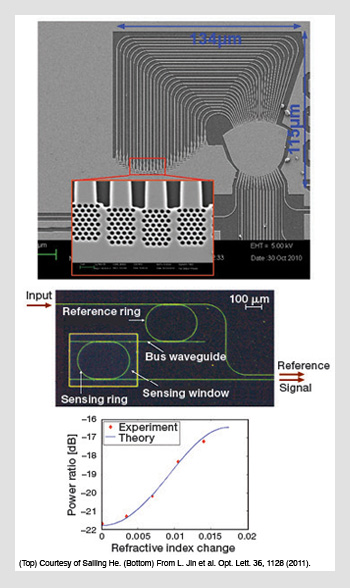 Arrayed waveguide grating (de)multiplexers and double-ring sensors. (Top) Fabricated reflective arrayed waveguide grating (de)multiplexer with 8 x 400 GHz channels. (Center) Optical microscope image of the double-ring sensor fabricated on a silicon-on-insulator substrate. The two rings have slightly different free spectral ranges. The chip size is only 1.3 x 0.7 mm. (Bottom) Normalized output power versus the sample refractive index change when a broadband source with 28 nm bandwidth centered at 1,553 nm was used. (Top) Courtesy of Sailing He. (Bottom) From L. Jin et al. Opt. Lett. 36, 1128 (2011).
Also at Zhejiang University, one of us (Jian-Jun He) has been working on novel semiconductor lasers and photonic integrated devices. Recently, his group proposed and experimentally demonstrated a digitally wavelength-switchable laser based on V-coupled cavities employing the Vernier effect. The fabrication process and chip size are similar to those of a Fabry-Perot laser, without complex gratings and multiple epitaxial growths. Single-electrode-controlled digital wavelength switching over 16-channels with 100 GHz spacing has been demonstrated, with a side-mode suppression ratio as high as 40 dB. Such a simple and potentially low-cost wavelength-switchable laser has great potential for applications in optical networks and beyond.
Jian-Jun He’s group also proposed and demonstrated a highly sensitive sensor based on two cascaded microring resonators that employ the Vernier effect. By coupling the light from a broadband source such as a light-emitting diode (LED) into the input-port and detecting the power ratio between the signal and reference ports, He’s group has demonstrated a highly sensitive intensity-interrogated sensor. The elimination of the requirement for an external bulky and expensive tunable laser or spectrometer will pave the way for low-cost practical applications of planar waveguide ring-resonator biosensors.
Integrated photonics research in Hong Kong
Academics in Hong Kong, a special administrative region of China, have also been playing major roles in integrated photonics research as well. Under China’s “One Country, Two Systems” policy, Hong Kong research programs are largely separate from those in China. In Hong Kong, basic research programs are funded under the Research Grants Council, while applied research programs are funded under the Innovation and Technology Commission. Here, we highlight integrated photonics research projects being carried out by researchers at the City University of Hong Kong (CityU) on polymer-based integrated photonics, and researchers at the Chinese University of Hong Kong (CUHK) and the Hong Kong University of Science and Technology (HKUST) on silicon photonics research.
Over the past 15 years, H.P. Chan and colleagues at CityU have been devoting their effort to the design and fabrication of practical polymer waveguide devices suitable for optical communication systems. These include variable optical attenuators, optical interleavers, optical cross-connect switches, optical splitters, vertical coupling polarization splitters and switches, polymer-based liquid crystal devices, long-period waveguide and Bragg grating devices, optical waveguide amplifiers, etc. In order to bring polymer-based planar lightwave circuit (PLC) devices closer to commercialization, Chan has also been focusing on studying the reliability of polymer materials, fabrication processes and packaging techniques. Specifically, he has developed a model to analyze the stress-induced birefringence effect in polymer-based waveguide devices in order to more accurately predict device performance.
One of us (Hon K. Tsang) at CUHK has worked on integrated photonics for nearly two decades and silicon photonics for more than a decade. Tsang’s group carried out some of the first measurements of Kerr nonlinearity, two-photon absorption and Raman gain in silicon. More recently, Tsang’s group demonstrated applications of silicon microring filters and modulators for access networks and RoF distribution, as well as the engineering of gratings for fiber-chip coupling for improved efficiency, bandwidth and polarization independence.
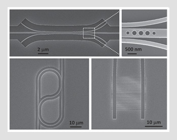
 Grating couplers. (Top) Apodized waveguide grating coupler between the optical fiber and the nanophotonic waveguide. The SEM images are of (bottom left) a focusing grating coupler, (bottom center) a subwavelength grating coupler and (bottom right) an apodized grating coupler.
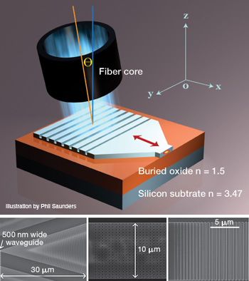
The shrinkage of silicon waveguide widths to below 500 nm has made it a challenge to efficiently couple light between the waveguide and a standard single-mode optical fiber. Tsang’s group adopted the surface-coupling approach, which uses waveguide gratings to diffract light into the silicon waveguide or output from the waveguide to an optical fiber. To reduce packaging costs, Chen et al. demonstrated a practical technique to realize vertical fiber coupling with linearly chirped gratings in order to reduce the back-reflection and attain a coupling efficiency comparable to that of the typical angled alignment approach. They also realized an apodized grating coupler, which attained one of the best coupling efficiencies experimentally reported to date, with a loss of only 1.2 dB attained using a coupler fabricated by electron beam lithography and a subwavelength grating coupler (which can be fabricated by the same etch step as the waveguides). The group showed how polarization-independent coupling may be achieved using subwavelength structures.
One of us (Andrew W. Poon) at HKUST has been spearheading silicon photonics research for nearly a decade. Poon’s group focuses on the design, fabrication and characterization of microresonator-based devices on silicon chips. The host of silicon photonic devices demonstrated on-chip optical interconnections and biosensing, including electro-optically reconfigurable add-drop filters, electro-optical switches and modulators, electro-optically reconfigurable delays, coupled-resonator optical waveguide delays, wavelength-selective sub-bandgap all-silicon photodetectors and microparticle add-drop devices.
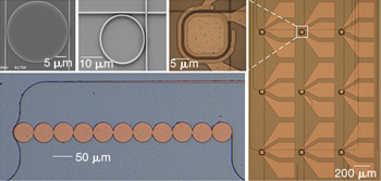 Microresonator-based devices fabricated on silicon chips. SEM and optical micrographs of some representative microresonator-based devices fabricated on silicon chips at Nanoelectronics Fabrication Facility of the Hong Kong University of Science and Technology. (Top, from left) SiN microdisk, SiN microring, silicon-on-insulator microring switch. (Right) silicon-on-insulator microring switch matrix. (Bottom) SiN microdisk coupled-resonator optical waveguide.
Poon’s group has exploited both SOI and deposited SiN on silica substrates. The Nanoelectronics Fabrication Facility of HKUST, a fully equipped facility for 0.35-mm complementary metal oxide semiconductor processes, fabricated all of their devices. Recently, Poon’s group has been working toward III-V heterogeneous integration on silicon for active devices for on-chip optical interconnections. In collaboration with electrical engineer Kei May Lau of HKUST, Poon’s group and Lau’s team are investigating monolithic high-speed low-voltage small-footprint waveguide photodetectors by hetero-epitaxy of high-crystalline-quality III-V on silicon. In addition, Poon’s group and Huang’s group of the Institute of Semiconductors, CAS, have also started a joint venture to realize III-V-on-silicon unidirectional microcavity lasers, with the goal of demonstrating unidirectional laser emission in a silicon waveguide.
Future outlook
Looking ahead, we feel that the future seems bright for integrated photonics research in China. With many new technological challenges unfolding, there is plenty of room for integrated photonics researchers in China to contribute and hopefully take a leading role in the near to intermediate future. With the growing number of integrated photonics research groups over many major university laboratories and research institutions in China, and strong backing from the Chinese government, we are optimistic that the importance and impact of integrated photonics research in China will grow to a new height. Integrated photonics “made in China” is already here, but the best is yet to come. t
We gratefully acknowledge many research groups in China contributing their research highlights to this article, including Buwen Cheng, Qiming Wang, Wei Wang, Lingjuan Zhao and Ninghua Zhu of Institute of Semiconductors, CAS; Yi Luo and Changzheng Sun of Tsinghua University; Qihuang Gong and Zhiping Zhou of Peking University; Sailing He and Deren Yang of Zhejiang University; H.P. Chan of CityU; and Kei May Lau of HKUST. We also thank many of our former and present students, post-doctoral fellows and colleagues who contributed to this article and their research work highlighted here. These include H. Chen (now at Sun Yat-Sen University), X. Chen (now at Surrey University), C.W. Chow (now at National Chiao Tung University), C. Li (now at Institute of Microelectronics, A*STAR Singapore), X. Luo (now at Institute of Microelectronics, A*STAR Singapore), B. Xiong (now at Tsinghua University), L. Xu (now at Columbia University); Y.-F. Xiao, X. Hu and H. Yang of Peking University; S. Feng, T. Lei and H. Cai of HKUST.
Andrew W. Poon is with the department of electronic and computer engineering, HKUST, Hong Kong. Linjie Zhou, and Jianping Chen are with the State Key Laboratory on Advanced Optical Communication Systems and Networks, SJTU, Shanghai. Yong-Zhen Huang and Jinzhong Yu are with the State Key Laboratory on Integrated Optoelectronics, Institute of Semiconductors, CAS, Beijing. Jian-Jun He is with the Centre for Integrated Optoelectronics, State Key Laboratory of Modern Optical Instrumentation, Zhejiang University, Hangzhou. Hon K. Tsang is with the department of electronic engineering, CUHK, Hong Kong.
References and Resourcess
>>The 973 Program, China’s Major State Basic Research Development Program
>> The 863 Program, State High-Tech Development Plan
>> Y. Luo et al. “Very Simple Integrated DFB Laser / EA Modulator Utilizing Gain Coupling,” in Proceedings of the Tenth International Conference on Integrated Optics and Optical Fiber Communication (Hong Kong, 1995).
>> W. H. Wong et al. "Polymer Devices for Photonic Applications," J. of Crystal Growth 288, 100 (2006).
>> P.-F. Cai et al. “40 Gb/s AlGaInAs Electroabsorption Modulated Laser Module Based on Identical Epitaxial Layer Scheme,” Jpn. J. Appl. Phys. 46, L664 (2007).
>> X. Y. Ma et al. “Electrically Pumped ZnO Film Ultraviolet Random Lasers on Silicon Substrate,” Appl. Phys. Lett. 91, 251109 (2007).
>> X. Chen et al. “Fabrication-Tolerant Waveguide Chirped Grating Coupler for Coupling to a Perfectly Vertical Optical Fiber,” IEEE Photon. Technol. Lett. 20, 1914 (2008).
>> M. Wang et al. “Light Emission Properties and Mechanism of Low-Temperature Prepared Amorphous SiNX Films. I. Room-Temperature Band Tail States Photoluminescence,” J. Appl. Phys. 104, 083504 (2008).
>> D. Dai et al. “Highly Sensitive Sensor Based on an Ultra-High-Q Mach-Zehnder Interferometer-Coupled Microring,” J. Opt. Soc. of Am. B 26, 511 (2009).
>> D. Dai et al. “A Silicon-Based Hybrid Plasmonic Waveguide with a Metal Cap for a Nano-Scale Light Confinement.” Opt. Express 17, 16646, (2009).
>> N. Zhu et al. “Microwave Generation in an Electro-Absorption Modulator Integrated with a DFB Laser Subject to Optical Injection,” Opt. Express 17, 22114 (2009).
>> K. S. Chiang. "Development of Optical Polymer Waveguide Devices," Proceedings of SPIE 7605 (2010).
>> X. Chen et al. “Apodized Waveguide Grating Couplers for Efficient Coupling to Optical Fibers,” IEEE Photon. Technol. Lett. 22, 1156 (2010).
>> D. Dai et al. “Experimental Demonstration of an Ultra-Compact Si-Nanowire-Based Reflective Arrayed-Waveguide Grating (De)multiplexer with Photonic Crystal Reflectors.” Opt. Lett. 35, 2594 (2010).
>> D. Dai et al. “Low-Loss Hybrid Plasmonic Waveguide with Double Low-Index Nano-Slots.” Opt. Express 18, 17958 (2010).
>> T. Hong et al. “A Selective-Area Metal Bonding InGaAsP-Si Laser,” IEEE Photon. Technol. Lett. 22, 1141 (2010).
>> C. Sun et al. “40 Gb/s AlGaInAs Electroabsorption Modulated Laser Module with Novel Packaging Design,” in Proceedings of the 22nd IEEE International Semiconductor Laser Conference (Kyoto, Japan, 2010).
>> L. Wang et al. “40 Gbits/s All-Optical Clock Recovery for Degraded Signals Using an Amplified Feedback Laser,” Appl. Opt. 49, 6577 (2010).
>> S. J. Wang et al. “AlGaInAs/InP Microcylinder Lasers Connected with an Output Waveguide,” IEEE Photon. Technol. Lett. 22, 1349 (2010).
>> Y.-F. Xiao et al. “High-Q Exterior Whispering-Gallery Modes in a Metal-Coated Microresonator,” Phys. Rev. Lett., 105 (15), 153902 (2010).
>> Z. Zhou et al. “Silicon Nanophotonic Devices Based on Resonance Enhancement,” J. of Nanophotonics 4, 041001 (2010).
>> Y. X. Zhang et al. “5Gb/s Optical Logic AND Operations by Using Monolithically Integrated Photodiode and Electroabsorption Modulator,” Proc. of SPIE 7717, 77171B-1 (2010).
>> X. Chen et al. "Polarization-Independent Grating Couplers for Silicon-on-Insulator Nanophotonic Waveguides," Opt. Lett. 36, 796 (2011).
>> S. Feng et al.“Silicon Photonics: from a Microresonator Perspective,” Lasers and Photonics Reviews, 2011 (under review).
>> F. Hu et al. “Band-Pass Plasmonic Slot Filter with Band Selection and Spectrally Splitting Capabilities,” Opt. Express 19, 4848 (2011).
>> L. Jin et al. “Optical Waveguide Double-Ring Sensor Using Intensity Interrogation with Low-Cost Broadband Source,” Opt. Lett. 36, 1128 (2011).
>> S. Su et al. “GeSn p-i-n Photodetector for All Telecommunication Bands Detection,” Opt. Express 19, 6400 (2011).
>> X. J. Wang et al. "Extraordinary Infrared Photoluminescence Efficiency of Er0.1Yb1.9SiO5 Films on SiO2/Si Substrates," Appl. Phys. Lett. 98, 071903 (2011).
>> L. Zhou et al. "Coherent Interference Induced Transparency in Self-Coupled Optical Waveguide-Based Resonators," Opt. Lett. 36, 13 (2011).
>> L. Zhou et al. "Waveguide Self-Coupling Based Reconfigurable Resonance Structure for Optical Filtering and Delay," Opt. Express 19, 8032 (2011).