
Scatterings
Growing Lasers on Silicon
A group at The University of California, Berkeley, described a method of creating gallium arsenide nanolasers monolithically integrated onto silicon.
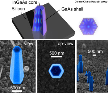 Tiny hexagonal pillars of GaAs/InGaAs grown on Si become subwavelength nanolasers.
Tiny compound semiconductor lasers grown directly on silicon surfaces could offer a route to combining optics with electronics. If microprocessor chips could depend on light, rather than electrons, to move data, they could eliminate the communications bottleneck that currently limits the efficiency of chip-to-chip (and sometimes even intra-chip) data transfers. Roger Chen and others in Connie Chang-Hasnain’s group at The University of California, Berkeley, recently described a method of creating gallium arsenide nanolasers monolithically integrated onto silicon. The lasers do not require further processing to form optical cavities and they emit at 950 nm at room temperature. (Nature Photon., doi: 10.1038/NPHOTON.2010.315 )
…Log in or become a member to view the full text of this article.
This article may be available for purchase via the search at Optica Publishing Group.
Optica Members get the full text of Optics & Photonics News, plus a variety of other member benefits.