
Optical Engineering
Evolving CMOS Technology for High-Performance Single-Photon Detection
For decades, solid-state detectors could capture individual photons. This is now possible to do using avalanche photodiodes. So-called single-photon avalanche diodes (SPADs) are avalanche photodiodes biased above breakdown in Geiger mode and fabricated using CMOS processes.
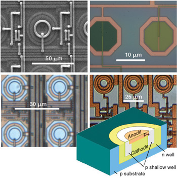 SPAD examples and (inset) a 3-D representation.
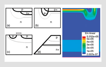 Common structures of CMOS SPADs. (Left) Premature edge breakdown prevention mechanisms in planar and semi-planar processes. (Right) A simulation of the electric field distribution around the guard ring of style (b). Note that the electric field is maximized in the anodic region and kept below the critical level for impact ionization in silicon on the guard ring.
The primary engineering challenge of SPAD fabrication is figuring out how to prevent premature edge breakdown at the sharp edges of implant boundaries, where the electric field is high. Proper doping can reduce this field, but doped regions must be carefully designed to prevent depletion regions that extend too far under the active region with high bias voltages, and to avoid doping differentials that are too small to prevent edge breakdown.
…Log in or become a member to view the full text of this article.
This article may be available for purchase via the search at Optica Publishing Group.
Optica Members get the full text of Optics & Photonics News, plus a variety of other member benefits.