
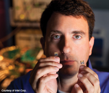
 Mario Paniccia holds the thin optical fiber used to carry data from one end of the 50 G silicon photonics link to the other.
It's all about data. The Information Age has become a digital explosion, with data growing exponentially at a rate of tenfold every five years. According to the International Data Corporation, the amount of digital information produced by humanity in 2020 will grow to 35,000 exabytes—3.5 × 1022 bytes, and 44 times more than was produced in 2009.
Moving all of this data around the Internet, within data centers, in and around PCs and servers, and between chips inside computing devices will require the widespread adoption of optical communications in order to scale with the growth in storage and computing demands. The barriers to the eternal promise of ubiquitous fiber optics has always been cost, and today optics only wins for the niche of applications that demand very long distances or unusual levels of performance that simply can't be achieved using copper wires.
Just as with the evolution of the integrated circuit, optics' pathway to mass markets will entail replacing today's discrete and bulky technology with integrated, silicon-based photonics. The recent development of hybrid silicon lasers has eliminated a major barrier to producing fully integrated transceivers using the same silicon high-volume-manufacturing tools used to fabricate billions of computer chips each year. (See related article on silicon photonics in May 2010 OPN.) These are the same processing techniques that have made integrated circuits so successful that, in less than half a century, we find them controlling nearly everything we touch on a daily basis: our cars, our televisions, our music players, and of course the entire fabric of the Internet.
To validate this viability of integrated silicon photonics, we developed a fully integrated end-to-end silicon photonics link. This research is separate from Intel's new Light Peak technology, though both are components of Intel's overall I/O strategy. Light Peak is an effort to bring a multiprotocol, 10-Gbps connections to Intel client platforms. Silicon photonics research aims to use silicon integration to bring dramatic cost reductions, reach terascale data rates, and bring optical communications to an even broader set of high-volume applications.
The result of this research, announced this past summer, is the 50-Gbps silicon photonics link. This link demonstrates all of the components that are necessary to develop viable silicon photonics products in the future. This includes not only the silicon chips themselves, but packaging consistent with high-volume manufacturing, assembly and connectorization. In addition, we sought to demonstrate bandwidth scalability with wavelength-division multiplexing, and to show a path to low-cost, terabit-per-second optical links to meet the challenge of the information explosion.
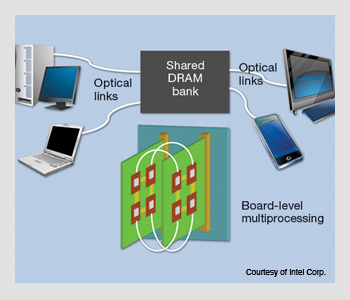 Low-cost optical interconnects will remove distance constraints for high-bandwidth I/O, providing new options for system designers.
A wealth of data
Before describing the details of our 50-Gbps link, it is useful to take a few moments to appreciate the phenomenal flood of data at hand. This torrent of bits is the result of several technological developments, starting with the growth of the Internet itself. Nearly 2 billion people use the Internet, a figure that continues to grow rapidly. In 2014, the Internet will be four times larger than it was in 2009. Internet usage models have also expanded, enabling everything from cloud and cluster networks to Web-enabled, data-hungry consumer applications such as video on demand.
Companies have taken advantage of the Internet and its capacity to collect, share and generate information. Businesses from manufacturing and finance to health care and travel now rely on massive quantities of data to fuel their operations. Large retailers, for example, handle as many as a million customer transactions every hour, feeding databases estimated at more than 2.5 petabytes—167 times the storage of the books in America's Library of Congress. Furthermore, information begets information. Databases such as these feed analytical engines to deduce trends on customer buying habits or trends in massive scientific datasets—a process that in turn produces yet more data to share and store.
Consumers also contribute to the data explosion. Masses of people are creating and sharing content on social networks as part of their daily routine. The most notable impact to networks is with video. According to the Cisco Visual Networking Index, video already accounts for more than a third of consumer Internet traffic. This will grow to 90 percent by 2014, with HD and 3-D video accounting for nearly half of this traffic, and with applications such as video conferencing and live streaming video rapidly growing as well.
Inevitably, this wave of data crashes upon the individual computer systems that need to make sense of the bits and bytes, systems whose computational demands are becoming increasingly I/O limited. Multicore processors are packing more computing capability into smaller spaces. Within a server chassis, these high-performance processors are constrained both electrically and physically. As the demand for higher data rates increases, traditional copper channels require a closer proximity to processors, memory and I/O. This limits both the number of memory channels and the number of memory modules per channel, affecting bandwidth efficiency and capacity per processor socket.
Rethinking systems designs
Optical interconnects will become a game changer if we can combine the high data rates, reach and integration of multiple photonic channels with prices that are practical for system-level interconnects. Eliminating the constraints of power and distance would provide the flexibility to revolutionize system-level architecture. Servers would be able to expand memory beyond what is physically and electrically feasible by connecting to remote, optically attached memory systems without sacrificing speed, thus maximizing both delivered bandwidth and capacity. Data centers would be able to maximize the performance of multicore processors for such applications as large databases or virtualized environments.
For manufacturers, this capability could lead to "hyperdocks." Imagine plugging an ultrathin laptop into an office docking station that immediately gives it the performance of a high-end work station through direct connections to additional memory and coprocessors. Or consider the future of video displays. Today 1080p seems sufficient on most TVs—but imagine a screen that fills your entire wall, something you often see in science fiction stories, and using that wall for a 3-D video conference in which the other party literally appears to be in the room with you.
To keep the same quality and resolution, you might need 16 times the pixels of today's HDTV. Transmitting such "ultrahigh-definition" images at a 60-Hz refresh rate requires 60 Gbps, which is beyond what we can do with copper but is easily accomplished with fiber optics. The problem is doing it economically with fiber optics.
 Intel Labs' 50 Gbps silicon photonics link.
Realizing silicon photonics
Before the turn of the millennium, silicon photonics remained an unlikely candidate for fiber optics. Because silicon is optically transparent at key optical communications wavelengths (around 1,310 and 1,550 nm), it could be used to create waveguides and other passive devices but little else. Silicon lacked the necessary physical properties for active devices—specifically, the direct bandgap needed for light emission or the electro-optic (Pockels) effect typically used for the modulation of light.
Our goal has been to create active optical devices that can be integrated and fabricated using the same manufacturing equipment used to make silicon integrated circuits. Our vision included three phases of research and development: 1) to prove feasibility by demonstrating optical building blocks, then 2) to move to integration, and finally 3) to implement high-volume manufacturability. For the middle part of the past decade, we focused on phase I, developing a variety of fundamental building blocks such as photodetectors, lasers and modulators, and then scaling their performance to higher speeds.
It's a testament to the progress that has been made in this field to remember that, before 2004, such devices had not yet been demonstrated at speeds greater than 20 Mbps in silicon. Today speeds are measured in tens of gigabits per second, a viable silicon photonics industry has emerged, and we have been able to demonstrate not only 40 Gbps modulators, but 40 Gbps photodetectors, silicon Raman lasers and hybrid indium phosphide-silicon lasers.
Soon after, we shifted focus from the development of building blocks to phase II—integration. The 50 Gbps silicon photonics link is the product of that effort, and it required us to put devices with different process recipes onto a common substrate. While in phase I, we enjoyed the freedom to optimize processing to produce individual devices. The integration phase required the team to tackle the practical engineering challenges of consolidating process flows and considering the thermal effects that devices such as the lasers have upon neighboring devices.
Phase II included solving issues of packaging, assembly and fiber coupling, which contribute significantly to the cost of the final fiber-optic components. Many 10 Gbps transceivers today still require active, sometimes manual fiber alignment and assembly procedures. The silicon photonics industry needs to shift to fully automated, high-volume assembly techniques as used in the PC industry; otherwise, the cost benefits of silicon will be negated by pricy packaging.
Inside the 50 Gbps link
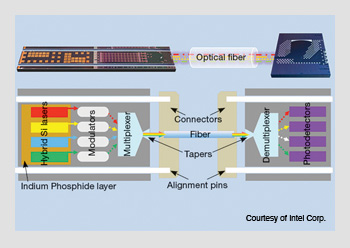
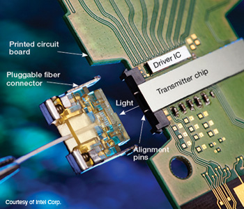
The 50 Gbps silicon photonics link is comprised of four basic components: a silicon photonics transmitter (Tx) chip, a silicon photonics receiver (Rx) chip, CMOS ICs (modulator driver, transimpedance amplifier) chips and a passive fiber-optic connector. These components are packaged and assembled on low-cost printed circuit boards. The link uses coarse wavelength division multiplexing, with each chip containing four optical channels operating at up to 12.5 Gbps per channel for an aggregate bandwidth of 50 Gbps on single fiber.
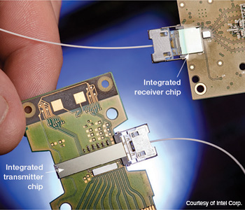
 The link's key silicon photonic elements, with the silicon photonic transmitter chip on the left and the silicon photonic receiver chip on the right.
Hybrid silicon lasers
One of the most challenging but important technologies in the link is also the basis of the transmitter—the aforementioned hybrid silicon laser. Developed by Intel and the University of California at Santa Barbara, a hybrid silicon laser consists of two elements: a silicon waveguide etched with distributed-Bragg-grating mirrors to form the laser resonator and an indium phosphide chip to act as a light emitter. The chip is bonded to the silicon by passing an oxygen plasma over the surface of both materials to form an oxide layer roughly 25 atoms thick. This oxide layer acts as the glue that fuses the two materials together. When a forward bias is applied to the indium phosphide, it emits photons into the silicon-waveguide resonator, where they accumulate and subsequently pass into the next silicon-photonic device.
We have monolithically integrated four hybrid silicon lasers onto a single silicon substrate with four traveling-wave optical modulators, a multiplexer and an inverted taper that couples light into a fiber. The four lasers were designed so that their wavelengths matched the ITU-T G.694.2 grid wavelengths of 1,291, 1,311, 1,331 and 1,351 nm.
The InP bonding can be done at the wafer level in the back end of the silicon processing flow. Therefore, hundreds or thousands of hybrid silicon lasers could be created from a single bond, enabling a high-volume path to light emission on a silicon photonics chip.
Traveling-wave modulators
After passing the output grating and exiting the laser resonator, the light enters a traveling-wave silicon modulator. The modulator shutters the light on and off to encode ones and zeros on the beam at rates up to 12.5 Gbps. There are two reasons for using these modulators rather than directly modulating the laser. First, at high data rates, modulating the laser directly would consume much more power. Second, direct modulation of a laser introduces chirp, which diminishes performance at high speeds. Since the long-term plan is to produce devices running at 40 Gbps per channel and beyond, this is essential for future scaling.
The silicon modulator relies on the free-carrier plasma-dispersion effect, in which silicon's refractive index is changed when the density of free carriers (electrons and holes) is varied. This modulation can be very fast, because free carriers can be swept out of the junction in approximately seven picoseconds. The speed is thus limited by the parasitic effects such as RC time constant limits. Accordingly, we adopted a traveling-wave scheme allowing the electrical and optical signal to copropagate across the device. To operate the traveling-wave modulator, our driver IC feeds a small RF signal into the transmission line, and the transmission line is terminated with an external resistor. We have shown in previous experiments that such modulators can have a 3-dB bandwidth of about 30 GHz and data transmission capability up to 40 Gbps.
 Packaging and assembly elements for the transmitter module.
Multiplexer
Light beams from the four modulators are combined into a single output beam with an optical multiplexer. Both the transmitter's multiplexer and the receiver's demultiplexer use an integrated optical grating. In the transmitter, this consists of a free-space region inside the chip where light beams reflect off the curved surface and the grating, and they are combined onto a single waveguide. The light then leaves the chip through a taper, a passive device that gradually changes the size of the optical beam to couple more efficiently into the optical fiber for transmission. An optical connector that includes a plastic lens and alignment pin couples light into fiber.
Demultiplexer
The optical signals are carried by a standard optical fiber and coupled into the Rx chip through a second optical connector. Signals travel into the demultiplexer to be separated once again into individual channels. The alignment of the wavelength channels between the hybrid silicon laser, the multiplexer and the demultiplexer is within one nanometer with only passive heat sinking.
PIN Photodetectors
An array of four photodetectors converts the photons back into electrons. We use germanium-on-silicon detectors to receive optical data because germanium is highly compatible with silicon IC manufacturing, and it detects light efficiently at the wavelengths emitted by the lasers. The challenge with these devices is minimizing the dark current due to crystal-lattice differences between germanium and silicon. For the 50 Gbps link, the measured 3-dB bandwidth of the four photodetectors was in the range of 9.4 to 10.6 GHz, with a measured responsiveness of approximately 0.9 A/W. As with the modulators, we have previously demonstrated that individual PIN photodetectors based on this technique can operate up to 40 Gbps.
Packaging and assembly
We packaged the Tx and Rx chips onto two different printed circuit boards. The system is designed to operate at 10 Gbps at room temperature with a passive heat sink. The Tx is "flip-chip" mounted to the substrate along with a silicon driver IC. Flip-chip bonding is the standard method of packaging modern microprocessors; it was developed as a high-speed alternative to wire-bonding. In this type of bonding, the silicon chip is flipped upside-down and placed on an array of solder bumps that form the connection between circuitry and the package.
The integrated receiver is flip-chip attached to a second substrate, which is copackaged with a commercially available four-channel receiver IC. Fiber coupling between the two chips is aligned passively with precise metal alignment pins seated into v-grooves in the silicon substrate. These pins allow the chips to mate with a hand-pluggable fiber connector containing a molded plastic lens assembly to direct light into the optical fiber.
Performance
The output power from the four hybrid silicon lasers, measured at the output of the integrated transmitter die, ranges from 2 to 9 mW. The transmitter has a rise/fall time of 41 to 44 ps, an extinction ratio ranging from 4.4 to 6.3 dB and a total jitter of 23 to 34 ps. We conducted bit error rate (BER) measurements at the data rate up to 12.5 Gbps per channel. These results are promising: With a data rate of 10 Gbps, we've been able to run the link for more than a day, transferring over 1 petabit of data, without errors, suggesting a BER of less than 3 × 10-15. We then increased the modulation speed and showed that individual channels could operate at up to 12.5 Gbps per channel with BER of less that 10-12. This puts the aggregate link speed at 50 Gbps overall.
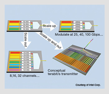 Paths to scaling the link data rates towards terascale performance.
Looking to the future
As we have seen with the IC industry, the value of integration comes not from combining a handful of transistors, but by putting millions of transistors together and scaling them to faster and faster speeds over time. Most fiber-optic technologies sold today are composed of several separate, discrete, optical components that are often hand-assembled to form an optical link. The successful multichannel integration demonstrated by this 50 Gbps link suggests that silicon photonics could further increase the number of parallel channels on each chip and scale to much higher data rates.
The day we saw the link reach 50 Gbps in the lab was both memorable and incredibly rewarding for the research team. However, at the same time it is only a stepping stone to much higher speeds. This integration platform provides us two vectors to scale performance. The first is to "scale up" the individual device speeds in the link. We have shown that we can run individual modulators and detectors to 40 Gbps, and we believe we can reach these speeds for the integrated link over time and perhaps reach even higher speeds. Simply doing so would enable us to reach 160 Gbps aggregate bandwidth with the same four channels.
We can also "scale out" by integrating more optical channels per chip, moving from 4 to 8 or 16 channels, for example. By combining both vectors, we easily envision delivering data rates of hundreds of gigabits per second, and ultimately more than a terabit per second from a single integrated silicon photonic chip.
This 50 Gbps link represents a huge step forward in our research, but there is more to be done as we take this technology from research to commercialization. On the silicon front, we will continue to optimize device performance. For the transmitter, we will push to drive modulators to operate at lower operating voltages to reduce power consumption as well as to maintain compatibility with ever-decreasing CMOS operating voltages (such as for 45-nm and 32-nm processes). We will also continue to improve the efficiency of the hybrid silicon laser and work to reduce the threshold voltage, again to minimize overall power consumption.
Looking to the coming century, every manufacturer of a connected device in the future should start thinking about how high-bandwidth, low-cost optical communications will benefit the products and services they deliver. Integrated silicon photonics is the start of bringing optical communications to anyone, anywhere around the world using optical communications. We are just at the beginning.
Sean Koehl, Ansheng Liu and Mario Paniccia are with Intel Labs in Santa Clara, Calif., U.S.A.
References and Resourcess
>> Cisco Visual Networking Index, white paper PDF
>> L. Liao et al. "40 Gbit/s silicon optical modulator for high speed applications," Electron. Lett. 43(22), 2007.
>> T. Yin et al. "31 GHz Ge n-i-p waveguide photodetectors on silicon-on-insulator substrate," Opt. Express 17, 13965-71 (2007).
>> A.W. Fang et al. "Single-wavelength silicon evanescent lasers," IEEE J. Sel. Quantum. Electron. 15(3), May/June 2009.
>> The Economist, "Data, data everywhere," February 2010.
>> IDC. "2010 digital universe study," April 2010.