
Confucius once said: “Better a diamond with a flaw than a pebble without one.” However, recent studies have shown that a flawed diamond can be even more valuable than a perfect one. But not just any flaw will do: The careful control of the imperfections has propelled diamond to the forefront of solid-state quantum information science and promises to launch a raft of new technologies.
Perfect diamond has one of the widest bandgaps of any material, being completely clear from the ultraviolet into the far infrared. Any imperfections give rise to scattering, and such color centers have been studied for their gemological properties. Usually, imperfections are seen as detrimental; however, diamond’s unique combination of properties—its clarity, hardness, thermal conductivity and Debye temperature—mean that single, isolated color centers can have properties that we usually associate with trapped single atoms, rather than with solid-state emitters.
One center in particular has raised our expectations of the application of diamond to quantum and biological technologies: the negatively charged nitrogen-vacancy center (NV). Experiments with NV have shown that it possesses an unprecedented range of properties. Optical properties of NV include high brightness, photo-stability and a nonlinear optical response—which allows for biomarking, single-photon and nanoscopy applications. In the quantum spin regime, NV shows room-temperature spin polarization and single-spin readout and room-temperature quantum coherence. In addition, it can be used to entangle nuclear and electronic spins, which have made NV an important driver for room-temperature quantum information processing applications.
Perhaps most remarkably, accessing this unique combination of properties is relatively inexpensive. Observing it requires little more than a laser, a microscope, a radio-frequency power supply and an avalanche photodiode. For its unique combination of properties, NV in nanodiamond has provoked an explosion of interest worldwide.
Here we highlight some of the remarkable properties of NV that have made it so attractive for key emerging technologies. We also review fabrication methodologies and some of the applications that promise to transform many fields of science, including single-photon experiments, magnetometry, decoherence sensing and biomarking. We will only discuss the negatively charged NV center, and not the neutral NV0 center, since only the negatively charged form seems practical for most quantum applications.
Fabricating NV in nanodiamond
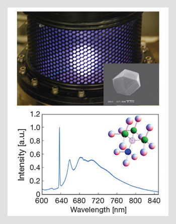 Nanodiamond growth and spectrum: (Top) Microwave plasma reactor used to grow diamond and incorporate NV centers. (Inset) A scanning electron microscope image of a diamond crystal hosting a single NV defect. (Bottom) Photo-luminescence spectrum from an NV center at 77 K, consisting of a zero phonon line at 637 nm accompanied by a broad phonon side band, which extends to 850 nm. (Inset) The NV structure. Nitrogen is represented by the blue sphere, the nearest-neighbor carbon atoms by the green and the other spheres represent the rest of the diamond lattice.
There are three main routes to creating NV: forming NV during the diamond growth process; activating N present in the diamond as an impurity; and implanting nitrogen into ultra-pure (low-nitrogen) diamond. Each method has its own advantages, and the choice of the fabrication methodology ultimately depends on the desired application.
The incorporation of nitrogen during the chemical vapor deposition (CVD) growth of nanodiamond crystals can be achieved by introducing nitrogen into the diamond growth mixture of methane and hydrogen. However, usually there is sufficient residual nitrogen present in the growth chamber to create NV. These crystals can then be manipulated and transferred to another position in order to be integrated into a practical device that uses a single NV center in nanodiamond.
Detonation nanodiamonds are formed from high-energy explosives that contain carbon and nitrogen. The key advantages of this method are that the average particle size of the nanodiamonds is approximately 3-6 nm—which is ideal for bio-applications—and the material is available on a large scale (hundreds of kilograms). However, the yield of available NV can be problematic.
Last, NV centers can also be formed in nitrogen-containing diamond powder. This powder generally originates from crushing high-pressure, high-temperature diamonds. The powder is then irradiated with high-energy radiation (e.g., protons, electrons or alpha particles) to introduce vacancies. Upon annealing above 700° C, the vacancies migrate toward the nitrogen, and the NV centers are formed.
Electronic structure
The NV center comprises a single substitutional nitrogen atom next to a vacancy in the diamond lattice. The NV center has six unpaired electrons—five from the neighboring carbon and intrinsic nitrogen, plus an additional electron trapped at the defect to form the negatively charged state of the center. Since NV has an even number of electrons, the many-electron configurations can form the spin triplet states (3A2 and 3E) and spin singlet states (1E and 1A1). The identification of the strong optical zero phonon line (ZPL) with the 3A2→3E transition as well as the ordering of the triplet states is now well established. The energetic ordering of the “dark” singlet states is still contentious. The figure below on the right depicts the currently accepted electronic structure.
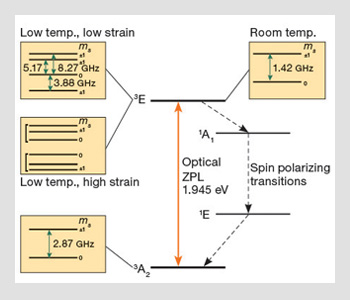 Electronic level structure of negatively charged nitrogen-vacancy center: The boxes depict the fine structure of electronic states for different temperature and strain regimes. Red and blue solid arrows indicate the allowable optical and magnetic transitions, respectively. Dashed black arrows show the sequence of transitions believed to be responsible for the optical spin-polarization of the ground state triplet.
The electronic fine structure of NV arises due to spin-orbit interaction and electronic spin-spin interactions, and is shown within the boxes of the figure. The ground 3A2 triplet exhibits a zero-field splitting of around 2.87 GHz between the spin sub-levels. The ground state fine structure exhibits both Zeeman and a weak Stark effect, and transitions can be driven via resonant RF fields.
The fine structure of the excited 3E state depends on both temperature and strain. At room temperature, the fine structure of the excited triplet mimics that of the ground triplet state with a single zero-field splitting of 1.42 GHz. At low temperatures, the fine structure of the excited triplet is highly dependent on crystal strain. In the low strain limit, it exhibits four fine structure levels corresponding to different combinations of orbital and spin sub-levels. The excited triplet fine structure shows pronounced Stark shifts—which may be important for tuning centers—for example, for cavity quantum electro-dynamic applications.
The observed optical spin-polarization of the ground triplet state is one of NV’s most remarkable properties. Under off-resonant illumination, population is transferred from the ms=±1 spin sub-levels to the ms=0 spin sub-level of the ground triplet state, so that the center is rapidly prepared in the ms=0 state with high probability. This same spin-dependent pumping also gives rise to different fluorescence rates from the ground states, so that fluorescence from the ms = ±1 states is significantly less than that from the ms=0 state. This mechanism allows for room-temperature, single-spin readout—which has made NV so important for quantum applications.
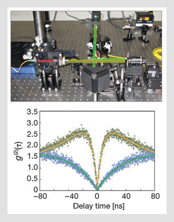 Measuring single photon emission from diamond: (Top) A scanning confocal microscope is used to excite and collect light emitted from single nitrogen-vacancy defects in diamond. (Bottom) Typical second-order correlation function for a single NV center in nanodiamond at two different excitation powers. The photon bunching at high pump powers (green dots) is attributed to a "shelving" state.
The complete mechanism that enables spin-polarization is not yet fully understood. Still, the required sequence of transitions can be inferred from the electronic structure model. For there to be a significant difference in the optical emission from the excited triplet spin sub-levels, there must be competing transitions that preferentially depopulate the ms = ±1 states.
The strongest competing non-radiative transition is believed to involve an intersystem crossing (ISC) from the excited triplet to the 1A1 state, which subsequently decays radiatively and non-radiatively to the 1E state. Given this decay of ms=±1 population to the 1E state, there must be a final non-radiative transition that also involves an ISC from the 1E to the ms=0 sub-level of the ground 3A2 state for the ground triplet state to spin-polarize. Hence, population is transferred from the ms=±1 to the ms=0 sub-levels of the ground triplet state via the intermediate singlet states.
Given the nature of the ISCs, these processes are expected to be both strain- and electric-field dependent, as has been observed in single crystal studies. Furthermore, this dependence might explain the variations in the observed spin polarization between NV centers.
Single photon sources
The first application we discuss does not use most of its unique properties, but only NV’s bright room-temperature fluorescence and single-center fabrication. NV is a practical and robust single-photon source.
Although for most optical technology, the photon nature of light is not evident, there is a growing range of applications that requires quantum effects. One such application is quantum key distribution. In particular, the BB84 protocol depends on sources that emit one, and no more than one, photon per excitation cycle. Such statistics cannot be obtained from an attenuated conventional source—for example, a laser. An attenuated source can only give an average intensity in photons per pulse—which is always limited by Poissonian statistics. By contrast, an isolated emitter must perforce emit single photons from a transition.
The NV center has negligible non-radiative relaxation from the excited state (after preparation in the ms=0 state) and does not photo-bleach. These properties make NV an excellent single-photon source. Photon emission is usually triggered by a green laser, typically 532 nm, and the emitted photons are collected using a high numerical aperture lens (typically in room-temperature experiments this might by 0.95) through a high-pass filter.
In practice, one must always confirm how well a source acts as a single-photon source. Source verification is performed by measuring the second-order autocorrelation function using a HanburyBrown and Twiss interferometer. This comprises a 50:50 beam splitter with output ports directed to two single-photon detectors. By routing the detector output to the start and stop inputs of a time correlator card, one can build up a histogram of time delays between consecutive single-photon events.
With appropriate normalization, it is possible to deduce the second-order autocorrelation function g(2)(τ). The signature of a true single-photon source is anti-bunching—i.e., the number of coincidences at zero delay between photon detection events is zero, so that g(2)(0)=0. Small deviations from zero can be attributed to experimental imperfections, including background fluorescence and non-ideal detectors. However, if there is more than one emitter, then g(2)(0)>0.5. For an ideal source of n emitters, g(2)(0)=1-(1/n), so g(2)(0)<0.5 is required before a single-photon source can be claimed.
An accurate determination of the second-order correlation function also enables the determination of many of the photophysical properties of the emitter. For example, the bunching signal seen in NV centers at high excitation powers is attributed to the existence of a “shelving state” that corresponds to the singlet transition providing the mechanism for spin polarization. Indeed, examining the autocorrelation functions and fitting to standard results confirms that the excited state lifetime is roughly 12 ns, and that the effective lifetime of the singlet system is about 130 ns.
The Weinfurter and Grangier groups made the first report of the anti-bunching of isolated NV centers in type Ib synthetic untreated diamond in 2000. Both groups demonstrated the simplicity of the system compared with previous atom-based single-photon sources and noted its potential for quantum key distribution. Single photons from NV in 40-nm nanodiamonds were reported in 2001, again by the Grangier group, who also demonstrated quantum key distribution with NV in nanodiamond in 2002.
The use of nanodiamonds, rather than bulk single crystal, allows for a better collection efficiency of the photons. This efficiency enhancement arises because the subwavelength size of these NDs mitigates the effects of refraction so that the nanocrystal acts as a point source for emitting light in air. In the bulk case, the air/diamond interface serves to reduce the light that can be collected by free-space optics.
The initial demonstrations of single photons from nanodiamond NV used free-space optics, but technology often demands integrated fiber-based solutions. There have been many proposals to couple NV to fiber, including micromanipulation of nanodiamond on fiber cores, direct growth of NV on fiber endfaces and compact confocal setups. The Quantum Communications Victoria team has produced the first commercial NV nanodiamond single-photon source with measured single-photon rates as high as 900,000 counts/s—more than one order of magnitude better than the first NV single-photon sources and with unprecedentedly low g(2)(0) < 5 x 10⁻⁴.
Some of the microscopic properties of NV in nanodiamond vary from crystal to crystal, especially with respect to strain-related properties. One approach to building nanodiamond technologies is to select and use only those crystals with the desired properties. This can be achieved using a combination of scanning electron microscopy and confocal mapping followed by nanomanipulation. Importantly, the NV properties do not change following manipulation. In addition to placing nanodiamonds on fibers, this approach can be applied to scanning probes for magnetometry and optical structures such as cavities and plasmonic wires to enhance emission and photon capture.
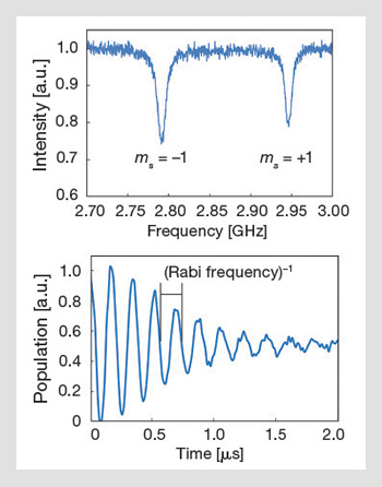 Optically detected magnetic resonance and Rabi oscillations: The ODMR signal arises because of the drop in fluorescence when the NV is in the ms = +1 or -1 states. Applying a small DC magnetic field lifts the degeneracy of the ms = ±1 states, and a resonant RF field takes population out of the optically pumped ms=0 state, thereby reducing the fluorescence signal. Coherent manipulation can also be done by pulsing the RF field; the figure on the bottom shows room-temperature Rabi oscillations that were obtained from a single nanodiamond NV center at room temperature.
Another emerging application of single-photon sources is in optical metrology—in particular, the push to define the quantum candela. The candela is currently characterized by calibrating the optical power of a light source against an equivalent electric heater. A potentially more accurate way of realizing the candela would be to use a deterministic single-photon source. The absorbed photon flux could then be determined with greater accuracy than for conventional sources due to reduced uncertainty in the number of emitted photons. As each photon carries a well-defined energy and the photon’s flux is known, photon counting becomes a very precise power measurement technique that could bridge the gap between conventional and quantum radiometry.
Although our focus here is on NV, the very broad emission of NV is a major limitation to its use in many fiber and daylight applications. For this reason, there is considerable effort being undertaken in exploring other centers with improved photophysical properties. There are a number of candidates, including nickel-, silicon- and chromium-related centers, all of which show single-photon emission, but with narrower spectral widths and often shorter lifetimes than NV.
Novel sensing with NV
The single-photon applications that we just discussed did not take advantage of the optical pumping and ground-state spin structure. However, these unique properties provide outstanding opportunities for sensing. Here, we briefly discuss two applications of NV for sensing, in magnetometry and decoherence sensing.
Researchers first demonstrated optically detected magnetic resonance on single NV centers in the late 1990s, and this forms the basis of most NV sensing schemes. Much of the development of such schemes was due to the work of the Wrachtrup group. By 2004, room-temperature single-center Rabi oscillations and decoherence times were measured (~0.6 µs). Since then, our understanding of decoherence mechanisms in diamond has advanced to the point where isotopically pure diamond material can be engineered with room-temperature electron spin decoherence times of 1.8 ms.
With NV showing unprecedented room-temperature quantum coherence, the time was ripe to explore the potential applications of this unique spin qubit. In 2005, Chernobrod and Berman envisioned a single-spin qubit with optical spin readout that would provide the basis for a new type of microscope—“the spin microscope”—and NV appears ideal for this application. In late 2008, the Wrachtrup and Lukin groups independently demonstrated NV magnetometry. The scheme works by detecting the Zeeman shift of spin levels using techniques adapted from nuclear magnetic resonance imaging. The sensitivity of the NV centers is ultimately limited by the ground-state decoherence time, and static DC and oscillating AC magnetic fields were detected with sensitivities down to 4 nT/√Hz.
The promise of a stable, well-characterized quantum system led Hollenberg and collaborators to describe an entirely new sensing paradigm: the decoherence microscope. Here, the quantum environment is explored by its effect on the coherence of the NV center. An application is to explore the randomly fluctuating weak magnetic fields associated with biological processes at the nanoscale. This novel form of quantum decoherence imaging is expected to have a profound impact on the nanoscale imaging of biological and complex systems, including single-ion channel switching, brain function and many more complicated systems.
Biomarking
The technology that allows scientists to directly image biological processes has started a revolution in our understanding of biology at the cellular and sub-cellular levels. However, commonly used fluorophores suffer from photobleaching and blinking—which limits their effectiveness. Other biolabels, such as quantum dots, are toxic and require encapsulation. Diamond is completely biocompatible and nontoxic, and—since NV is completely photostable—it is a promising biolabel.
One crucial parameter for the use of NV for biomarking is the size of the nanodiamond. To date, most experimental NV biomarking demonstrations were performed with nanodiamonds that were a few tens of nanometers in diameter. However, even smaller crystals can exhibit stable fluorescence; researchers have observed emission from NV in a single-digit nanodiamond. Remarkably, the luminescence from a single-diamond nanocrystal can be much brighter than standard fluorescent proteins.
Due to its photostability, it is also possible to track the ND’s trajectory in cells. Chang and co-workers demonstrated 3-D tracking of a single 35-nm nanodiamond over a micron range with confocal microscopy techniques. This result opens new avenues of exploration of NDs as drug-delivery vehicles and live imaging techniques at the nanoscale.
Chemical processes for functionalizing the surface of nanodiamonds with various carboxylic or other functional groups are under development. Then, through chemical reactions, the nanodiamonds can be conjugated with various drugs, vaccines or DNA. By attaching a specific reagent to the nanodiamond and tracking its motion, scientists will have the ability to probe biomolecules in vivo and to develop new chemical- and site-specific probes with nanometric resolution and beyond. This combination of the brightness and functionalized surfaces promises to place diamond at the center of the emerging field of functional nanoscopy.
Conclusions
Diamond is rapidly becoming the most effective platform for harnessing solid-state quantum physics. With the new ability to control all the quantum properties of a system, the next stage is to build technologies around it. This is one of the major goals of the 21st century: figuring out how to apply all of the properties of quantum mechanics toward the creation of new or enhanced technologies.
Nanodiamonds that contain nitrogen-vacancy color centers already appear center stage for this revolution. They represent the most convenient, controllable room-temperature quantum entity. Researchers around the world are incorporating nanodiamond NV in applications such as quantum key distribution, quantum-limited sensing and biomarking. It appears likely that this only captures a small fraction of the potential of this remarkable quantum platform.
The authors thank Lloyd Hollenberg, Steven Prawer and Andrew Tierney for useful discussions and helpful feedback with the manuscript.
A.D. Greentree, I. Aharonovich, S. Castelletto, M.W. Doherty, L.P. McGuinness and D.A. Simpson are with the School of Physics, University of Melbourne, Victoria, Australia.
References and Resources
>> A.M. Zaitsev. Optical Properties of Diamond: A Data Handbook, Springer, Berlin (2001).
>> A. Beveratos et al. Phys. Rev. Lett. 89 (2002).
>> G. Balasubramanian et al. Nature 455, 648-51 (2008).
>> Y.R. Chang et al. Nature Nanotech. 3, 284-8 (2008).
>> L.J. Rogers et al. New J. Phys. 10 (2008).
>> A. Krueger. Adv. Mater. 9999, 1-5 (2008).
>> I. Aharonovich et al. Nano Letters 9, 3191-5 (2009).
>> J. Tisler et al. ACS Nano 3, 1959-65 (2009).
>> C. Bradac et al. Nature Nanotech. 5, 345-9 (2010).
>> J.H. Cole and L.C.L. Hollenberg. Nanotech. 20, 495401 (2009).
>> I. Vlasov et al. Small 6, 687, (2010).