
Optical lithography is the engine that has powered the semiconductor revolution. It has proven to be flexible and adaptable, and, for more than three decades, it has met the semiconductor industry’s ever-
tightening requirements.
And yet, lithographers, managers and forecasters continue to fret that optical lithography may be facing its demise. In early 2002, one of the more forward-looking experts in the field stated that: “Without some invention that significantly changes the way optical lithography is practiced, a next-generation lithography technology—such as extreme ultraviolet lithography or electron projection lithography—will be required to extend the roadmap to the 45-nm node and beyond.”
Over the past year, the 45-nm threshold was crossed without fanfare, and the industry is pressing toward the 32-nm node, although experts are still worried about the need for some form of next-generation lithography. Of course, optical lithography today is indeed practiced differently than it was in 2002, but this is only proof of its robustness as well as our limited ability to predict its evolution.
The International Technology Roadmap for Semiconductors (ITRS, or The Roadmap) has become a well-respected forum for listing and updating lithography requirements. It is sponsored by the five leading chip manufacturing regions in the world: Europe, Japan, Korea, Taiwan and the United States. Its goal is to ensure cost-effective advancements in the performance of the integrated circuits and the products that use them. Its milestones, the “nodes,” are the half-pitch of the smallest dimensions that need to be patterned in every generation of microelectronic devices.
The industry has followed an impressive path; it has continually reduced the half-pitch approximately 1.43 every three years. This uninterrupted improvement is part of “Moore’s law,” which was named after Intel co-founder Gordon Moore and states that the number of transistors that can be placed inexpensively on an integrated circuit will double every two years. Moore first put forth this concept in 1965 as a prediction for the next 10 years.
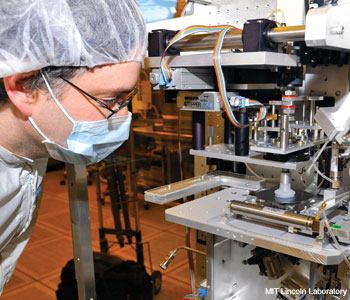 A 157-nm interference lithography system, which was designed and built at MIT’s Lincoln Laboratory, and which was used to pattern the dense gratings shown on pp. 2-3.
As I noted earlier, the 45-nm node is already in manufacturing as of 2010. According to the ITRS, the future nodes are expected to be:
-
32 nm in 2013
-
23 nm in 2016
-
16 nm in 2019
-
11 nm in 2022.
The strength of optical lithography lies in its large degree of parallelism, which translates into high manufacturing throughput and relatively low cost. The emphasis here is on the term “relatively.” The high throughput and low cost—and hence the low cost per pixel—must be evaluated in comparison with those of the alternative technologies, in other words, the next-generation lithography technologies such as extreme ultraviolet lithography or electron projection lithography.
State-of-the-art optical lithography tools carry a hefty price—more than $40 million each—but they are able to pattern 200 wafer-levels per hour at a resolution of 38 nm. Since these are 300-mm-diameter wafers, the throughput is approaching the phenomenal rate of 2 × 1012 pixels per second. Currently, no other lithography is capable of matching this enormous throughput.
With these impressive performance levels, one wonders if the experts’ concerns about optical lithography have been misplaced. The answer is “no.” There has been valid reason for concern, the main one being that optical lithography simply cannot keep up with the demands on resolution.
A roadmap of optical lithography to 38 nm
Since around 1980, reduction-projection optical lithography has been dominant. In this technique, the features on a photomask are imaged onto the wafer, typically at a 4:1 reduction ratio. Even with a perfect, aberration-free imaging system, there is a minimum feature size that can be printed, CDmin (for “critical dimension”), defined by diffraction:
CDmin ~ k1 λ/NA.
In this expression, λ is the vacuum wavelength, NA is the numerical aperture of the imaging system (not larger than n, the index of refraction of the medium in contact with the wafer), and k1 is a proportionality factor that is not less than ¼. In the past 20 years, all three quantities have been modified to reduce CDmin:
-
NA has grown from 0.5 to 1.35
-
λ has been reduced from 365 to 193 nm
-
k1 has been reduced from 0.7 to 0.27.
This combination has led to a dramatic reduction in CDmin: CDmin has shrunk from 500 to 45 nm.
How much further can optical lithography be pushed to meet the resolution requirements? Let us examine each of the quantities involved.
NA: The numerical aperture is as high as it is today because of the adoption of a technology that was considered impractical until a few years ago—liquid immersion lithography. Here, the space between the optical system and the wafer is filled with a transparent liquid of index n, reducing the effective wavelength, or alternatively increasing the numerical aperture. Today’s immersion systems use water, which at the operating wavelength of 193 nm, has n193nm = 1.44, leading to NA = 1.35.
Until late 2008, it appeared that further increases in NA could be obtained by introducing liquids with higher index. However, the trade-off between high-index and low-absorbance proved to be too challenging: Transparent single-component organic liquids were prepared and tested, but their index was no higher than about 1.65, affording a relatively small gain in CDmin; thus, these liquids were considered not worth the investment. Suspensions of higher-index nanoparticles were also considered but deemed to be fraught with too many technical risks.
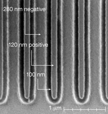 Initial demonstration of a dual tone photoresist: One exposure in one layer is followed by one development. The lithography was obtained with a relatively low-resolution stepper operating at 248 nm with a 0.6 NA, using a binary photomask with 250-nm half-pitch (at the wafer plane). The regions of 120 nm, 100 nm and 280 nm correspond to low-, intermediate- , and high-exposure dose, respectively (T. H. Fedynyshyn et al., unpublished, 2007).
λ: For several years (1997-2003), it seemed that reducing the wavelength was the preferred path. Much progress had been made in 157-nm lithography, from laser sources to optical materials to photoresists. Ultimately, however, several materials challenges— coupled with the economics of crystal growth—led to the abandonment of 157-nm lithography in favor of liquid-immersion 193-nm lithography. For a brief period, even shorter wavelengths were explored, such as 121.6 nm. However, none proved to be practical, in part because of the unavailability of powerful radiation sources and in part because of the lack of transparent lens materials.
k1: This is the least well-defined parameter. It represents a combination of the effects of resolution enhancement techniques such as phase-shifting masks and off-axis illumination, as well as effects of improved photoresists and lower defects. All this progress has brought us asymptotically close to the theoretical limit of ¼.
If NA, λ, and k1 are all at or near their limits, what is next?
Extending optical lithography to 23 nm
The optics-trained reader will realize that the limit of ¼ on k1 applies only if we attempt to pattern the photoresist in a single step. However, if we relax this requirement, and we are willing to use several thin-film deposition and etch steps, and maybe even additional lithography steps, the final pattern can have half the pitch of the diffraction-limited value. Indeed, technologists have been working feverishly to develop various flavors of this so-called “double patterning.”
Some methods of double patterning require two spatially staggered lithography steps in two layers of photoresist. These methods have been nicknamed litho-etch-litho-etch or litho-freeze-litho-etch, depending on the details of the processing steps. Another technique requires only one lithography step but more thin-film processing. Since it involves the formation of sidewalls to the patterned photoresist, it is called, not surprisingly, self-aligned double patterning (SADP).
With SADP, photoresists have been patterned with an effective k1 =0.15—i.e., with half the period of (an already aggressive) pattern of k1 = 0.30. Yet another process requires only a single exposure but two different development steps, so that the photoresist regions that have been exposed to intermediate doses are removed by one developer, as in conventional lithography (positive tone), but the regions exposed to higher doses are left in place with a different developer (negative tone). If the photoresist and the developer are engineered carefully, a single exposure and a single development step may be sufficient to achieve the same effect by simultaneously taking advantage of positive-tone and negative-tone behavior in the same “dual-tone” photoresist!
Furthermore, if one desires more flexibility in the feature geometry but no multiple steps for deposition and etching, nonlinear photochemical reactions may be built into the photoresist, enabling spatially staggered multiple exposures in the same photoresist – hence the term “double exposure,” as opposed to double patterning. Some scientists have proposed such double-exposure schemes by relying on multiphoton absorption, or onthe addition of a reversible contrast enhancement layer or photochromic layer to the photoresist. Overall, this is a fertile area for research in the near future, with the clear potential to break the k1 = ¼ barrier and approach its half, k1 = 1/8.
To be sure, there are serious technical challenges that must be resolved. For instance, when more than one exposure is required, whether in the same photoresist or in multiple layers, any inaccuracy in exposure-to-exposure alignment immediately translates into CD nonuniformity, which can amount to more than 12 percent of the CD error budget. In addition, all of these strategies include a penalty in throughput and overall cost of ownership. Still, double-exposure/double-patterning is an evolutionary step for optical lithography, and therefore it is preferred by many practitioners of this art.
A combination of water immersion lithography at 193 nm and double-exposure/double-patterning will enable the extension of optical lithography to the 32-nm and 23-nm nodes. Is there hope for optical lithography past this point? Perhaps by extending double patterning into triple and quadruple patterning?
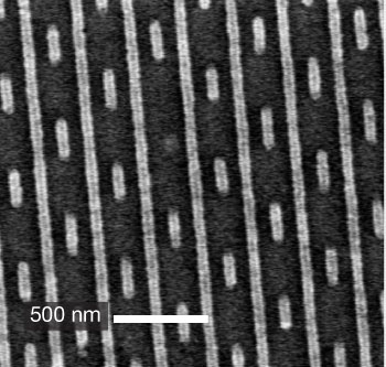
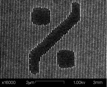 Composite pattern obtained by double exposure: Composite pattern obtained with two exposures in the same photoresist, followed by one development step. The first exposure formed the 45-nm half-pitch “carrier” grid using 157-nm interference lithography (without immersion), while the second provided the “modulation” cut-out pattern using a 248-nm, 0.6-NA stepper (from M. Rothschild et al., MRS Bulletin 30, 942-6, 2005).
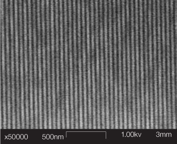 The highest resolution achieved with optical means: The highest resolution achieved with optical means: a grid with 22-nm half pitch, formed with immersion interference lithography at 157 nm (from T.M. Bloomstein et al. Opt. Express 14, 6434-43, 2006).
Towards the end of The Roadmap—11 nm
One lesson we have learned over the past decades is this: Extrapolating linearly from recent success is not necessarily a winning strategy. When the transition from 248-nm to 193-nm lithography gained momentum, it was natural to assume that further reducing the wavelength—this time to 157 nm—would provide the appropriate roadmap. It didn’t. Similarly, when liquid immersion lithography with water looked promising, it seemed reasonable to think that further increasing the fluid index would be the appropriate roadmap. That, too, failed.
So, although double patterning is certainly the current enabler of optical lithography, it would be risky to extrapolate again and assume that sub-23-nm half pitch can be achieved by further multiple patterning. Such processes are bound to run into severe practical limitations of alignment accuracy, deposition/etch uniformity and fundamental photochemistry.
So, although double patterning is certainly the current enabler of optical lithography, it would be risky to extrapolate again and assume that sub-23-nm half pitch can be achieved by further multiple patterning. Such processes are bound to run into severe practical limitations of alignment accuracy, deposition/etch uniformity and fundamental photochemistry.
There is another important component in lithography that is not captured by the expression for CDmin—the geometry of the desired pattern. Until recently, device designers and lithographers have operated in parallel worlds. The designers had free rein to choose the layout that would provide the best chip performance without regard to difficulties in patterning, while lithographers were asked to devise patterning methods for any arbitrary-shaped structure the designers fathomed. This paradigm has been changing.
In more and more organizations, the two teams have been coordinating their efforts, and the end product benefits both. They are converging towards layouts that fall on a regular underlying pattern or grid. Such geometries have been commonly used in memory cell design, but they are becoming more accepted also in microprocessors and even in application-specific integrated circuits (ASICs). While this trend is driven by considerations of cost and circuit performance, it also has important implications to lithography.
Electrical engineers will recognize the grid-based layout as consisting of a carrier frequency, the periodic grid that does not by itself contain information; and modulation frequencies, the “cut-out” or “trim” features, which provide the device’s spatial information. The highest resolution is required of the simple periodic grid formation, while the more complex patterns have somewhat more relaxed dimensional and positional requirements. To date, lithographers have been patterning both types of features with the same tools, even though they perform different functions. In the future, they may approach the two differently.
 Composite pattern obtained with hybrid lithography: Composite pattern obtained with hybrid lithography consisting of two exposures in the same photoresist, followed by one development step. The first exposure formed the 45-nm half-pitch “carrier” grid using 157-nm interference lithography (without immersion), while the second exposure provided the “modulation” cutout pattern using a 50-kV scanning electron beam lithography system (from M. Fritze et al., J. Vac. Sci. Technol. B 23, 2743-8, 2005).
The “modulation” will be performed with traditional projection optics at 193 nm, with water-immersion and double-exposure/double-patterning, thus printing down to at least 23 nm. However, patterning the carrier frequency can be achieved with a relatively simple interference system, since it does not require expensive general-purpose imaging optics or photomasks. Since the target is sub-23-nm half pitch, the interference will require liquid immersion, and the lithography step will be followed by double-exposure/double-patterning.
Although a full-fledged scanner can be used to define the periodic grid, an interference system provides cost advantages and more opportunities for resolution enhancement. In particular, fewer and simpler optical elements are required, there is no need for photomasks, and smaller working distances enable the use of more esoteric and/or slightly absorptive immersion fluids. In fact, using 193-nm liquid immersion interference lithography with high-index fluids, lithographers have already achieved 29-nm half pitch. Combining it with SADP, for instance, would bring optical lithography to the 16-nm node. The resolution record in interference lithography has been reported as 22-nm half pitch, albeit at the now discredited 157-nm wavelength and with a special immersion setup.
Nevertheless, a 157-nm interference system is much less daunting than a 157-nm scanner that requires unique photomasks, protective pellicles and large amounts of near-perfect crystalline calcium fluoride as lens material. A suitably engineered 157-nm interference system, when followed by double patterning, will bring optical lithography to the 11-nm node, which is as far as the ITRS is willing to forecast. This is predicted to occur more than a decade from now, in the year 2022.
In addition to helping projection optical lithography to remain a useful technology, interference lithography can also be a technology enabler in a different way. It can be coupled with electron beam lithography in a manner that takes advantage of the strengths of both. Electron-beam lithography has been practiced for many years because of its inherent high resolution, but its low throughput of a fraction of a wafer per hour has limited its use to research laboratories. Newer versions may enhance its throughput to 5-7 wafers per hour, which is still too low, even for many ASICs.
However, with gridded designs, much of the patterning can be accomplished with the fast interference lithography, leaving to the electron beam only the burden of patterning the cutouts. As with full optical lithography (interference lithography for the grid with projection optics for the cutouts), the hybrid optical-electron beam lithography decouples the carrier and modulation patterning, taking advantage of the respective strengths of each technology.
Such a system architecture provides flexibility in the choice of optical scanner vs. electron beam system for the modulation patterning, with the considerations being those of cost and throughput. For small batches of specialty chips, the less expensive electron beam system will be used, while for high volume production the high cost of the photomasks can be amortized over the full batch.
The road ahead
Optical lithography has come a long way since its early days. Consider that, 20 years ago, the smallest features printed with optical lithography were twice the wavelength used to print them; today, they are one-quarter of the wavelength. In the not-too-distant future, they will be one-tenth. New technologies have led to the evolution from short-wavelength lithography to phase shifting masks and from liquid immersion lithography to off-axis illumination. Further transformations, possibly combining double patterning and maskless interference lithography, may ensure its dominance for at least one more decade.
Many thanks to my colleagues at Lincoln Laboratory, especially T. Bloomstein, T. Fedynyshyn and M. Fritze, who insp-ired many of the concepts presented here, challenged some, and worked tirelessly
to validate others. This work was supported by the Defense Advanced Research Projects Agency under Air Force contract FA8721-05-C-0002. Opinions, interpretations, conclusions and recommendations are those of the author and do not necessarily represent the view of the United States Government.
Mordechai Rothschild is with Lincoln Laboratory, Massachusetts Institute of Technology in Lexington, Mass., U.S.A.
References and Resources
>> International Technology Roadmap for Semiconductors.
>> V. Liberman et al. J. Vac. Sci. Technol. B 20(6), 2567-73 (2002).
>> M. Rothschild et al. J. Vac. Sci. Technol. B 22(6), 2877-81 (2004).
>> M. Rothschild. Materials Today 4(2), 18-24 (2005).
>> M. Fritze et al. J. Vac. Sci. Technol. B 23(6), 2743-8 (2005).
>> J.H. Bruning. Proc. SPIE 6520, 652004-1 - 652004-13 (2007).
>> H. Sewell et al. Proc. SPIE 6520, 65201M-01 – 65210M-12 (2007).
>> C. Bencher et al. Proc. SPIE 7274, 72740G-01 – 72740G-10 (2009).
>> P.A. Zimmerman et al. Proc. SPIE 7274, 727420-1 – 727420-11 (2009).
>> T. L. Andrew et al. Science 324(5929), 917-21 (2009).
>> R. Gronheid et al. IEEE Trans. Circ. Syst. I 56(8), 1884-91 (2009).